Method of fabricating display device

a display device and a technology of a display device, applied in the field of fabricating a display device, can solve the problems of increasing the thickness of the leveling film, and achieve the effects of reducing the aperture ratio, avoiding the loss of light shielding pattern, and improving reflectan

Inactive Publication Date: 2005-02-17
SEMICON ENERGY LAB CO LTD
View PDF58 Cites 27 Cited by
  • Summary
  • Abstract
  • Description
  • Claims
  • Application Information

AI Technical Summary

Benefits of technology

An object of the present invention is to, by achieving all three purposes described above, fabricate a display device with a highly reliable wiring, a high aperture ratio and a uniform image. At the same time, the present invention has another object to improve the quality and reliability of electric appliances using the display devices fabricated in accordance with the present invention.
On the thus obtained flat surface, the breaking of wirings and the poor orientation of liquid crystal due to unevenness of the surface hardly occur. Moreover, the decrease in aperture ratio by providing a light-shielding pattern can be avoided. Furthermore, in a reflective liquid crystal display device, a reflectance is improved owing to reduced unevenness of the surface. The inventors of the present invention have found that the leveling rate is remarkably improved by using the present invention, satisfying all the above first to third requirements.

Problems solved by technology

However, since an etching process of a leveling film for forming a through hole therein should be easy for high productivity, there is a limit in increasing the thickness of the leveling film.

Method used


Image

  • Method of fabricating display device
  • Method of fabricating display device
  • Method of fabricating display device

Examples


embodiment 1

(Embodiment 1)

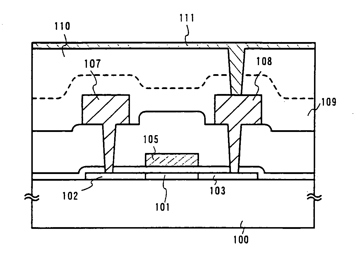
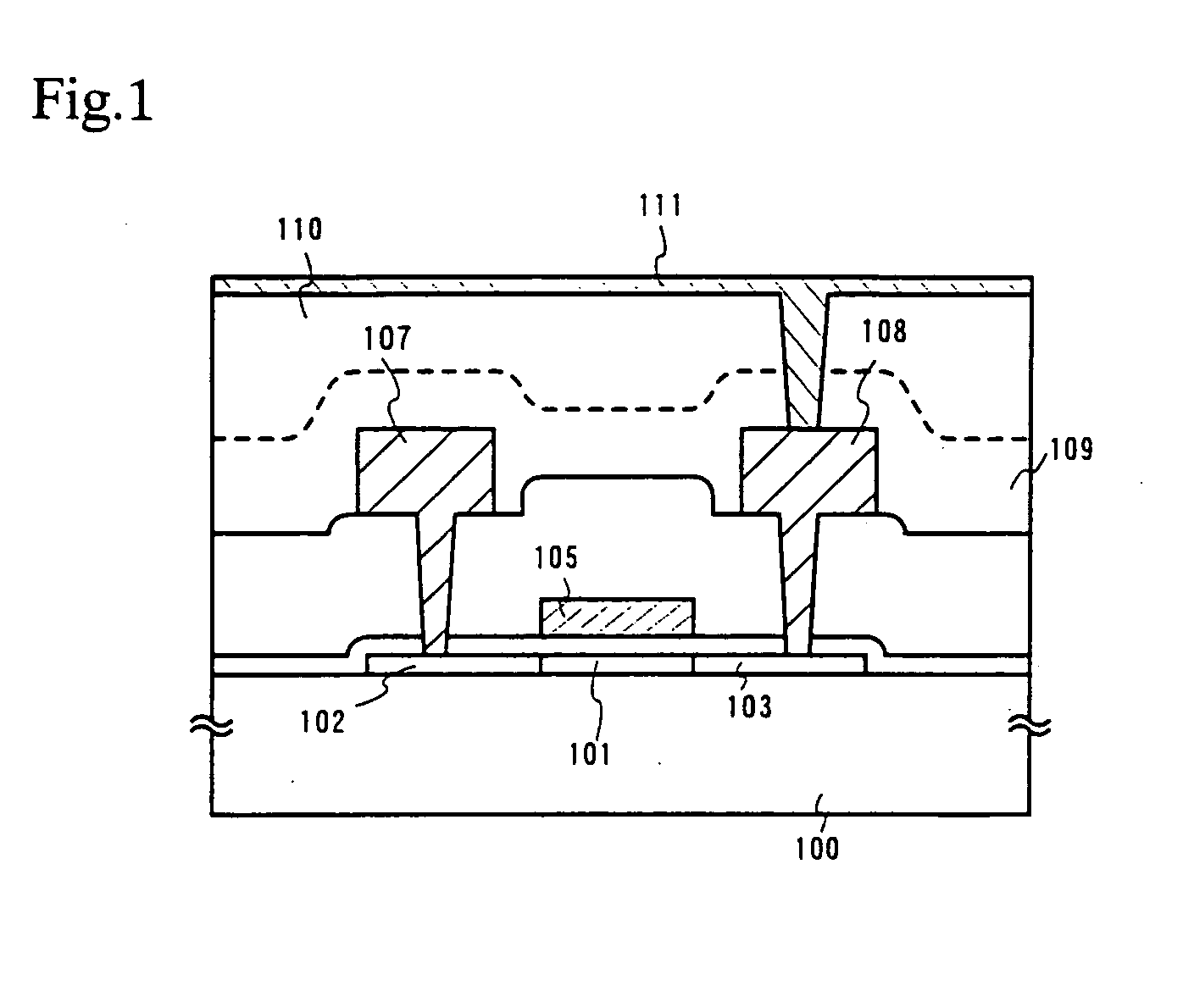
Embodiment 1 of the present invention will be described with reference to FIGS. 7A to 9C. A method of fabricating an active matrix substrate, particularly a pixel portion, will be herein described. The pixel portion includes a pixel TFT region that is a TFT provided in a pixel and a display region that does not include the TFT region.

In FIG. 7A, a glass substrate or a quartz substrate can be used as a substrate 700. A silicon substrate, a metal substrate or a stainless substrate on which an insulating film is formed may also be used for the substrate 700. A plastic substrate having a sufficient heat resistance can also be used.

Then, on the surface of the substrate 700 where a TFT is to be formed, a base film 701 made of an insulating film containing silicon is formed. In this embodiment, a silicon nitride oxide film having a thickness of 200 nm. is formed as the base film 701.

Successively, an amorphous semiconductor film (in this embodiment, an amorphous silicon...

embodiment 2

(Embodiment 2)

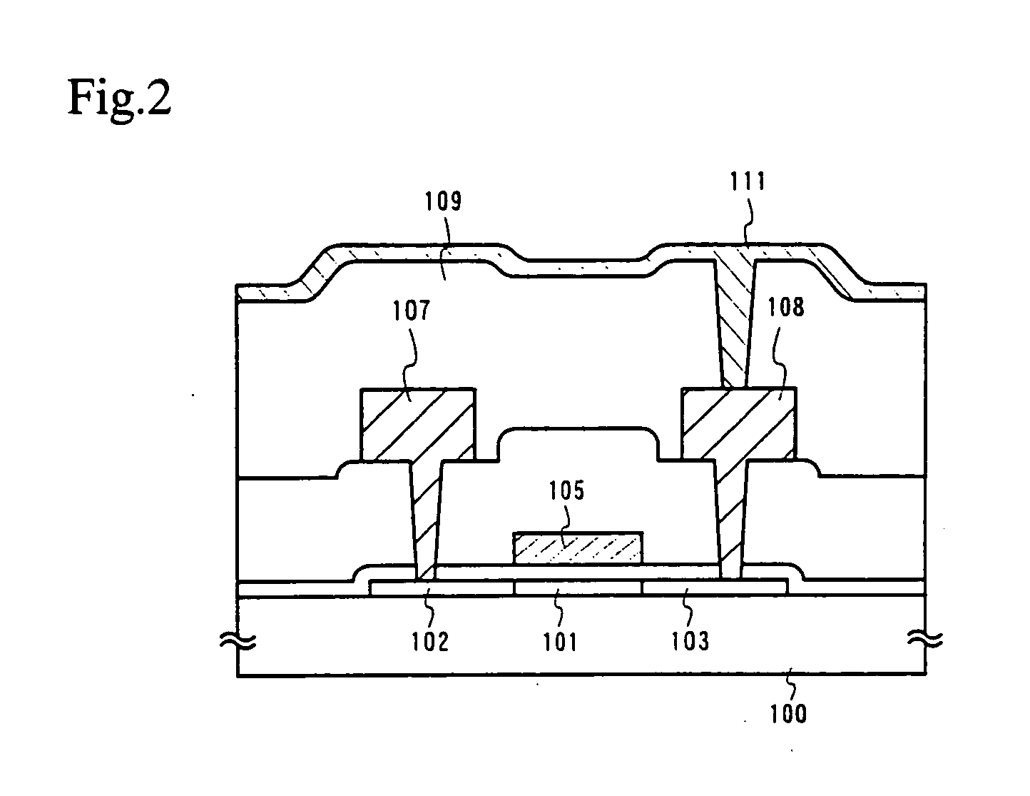
In Embodiment 2, the case where a pixel TFT having a different structure from that of Embodiment 1 is to be fabricated will be described. Since only a part of fabrication steps are different from those of Embodiment 1, the same fabrication steps are designated by the same reference numerals.

In accordance with the process of Embodiment 1, the fabrication steps up to the formation of the passivation film 718 are conducted. The first leveling film 719 is formed to a thickness of 0.3 μm (FIG. 9A). Then, the second leveling film 720 is formed to a thickness of 1.2 μm on the first leveling film 719. As the first leveling film 719 and the second leveling film 720, a polyimide resin, an acrylic resin, a resin containing a siloxane structure or an inorganic SOG material can be used. In this embodiment, an acrylic resin is used.

Since the first leveling film 719 has a thickness of 0.3 μm and the second leveling film 720 has a thickness of 1.2 μm, the total thickness of the f...

embodiment 3

(Embodiment 3)

In this embodiment, the steps for fabricating an active matrix liquid crystal display device using the active matrix substrate fabricated in Embodiment 1 or Embodiment 2 will be described. As shown in FIG. 10, an orientation film 1001 is formed on the substrate in the state shown in FIG. 9C. A polyimide film is used as the orientation film in this embodiment. For a counter substrate 1002, a counter electrode 1003 and an orientation film 1004 are formed. A color filter or a shielding film may be formed on the counter substrate as needed.

Next, after formation of the orientation films, a rubbing treatment is performed so as to orient liquid crystal molecules at a certain pretilt angle. Then, the active matrix substrate on which the pixel portion and driving circuits are formed is bonded with the counter substrate by a known cell assembling step through a sealing material or a spacer (not shown). Thereafter, liquid crystal 1005 is injected into a gap between the substra...


PUM

PropertyMeasurementUnit
thicknessaaaaaaaaaa
thicknessaaaaaaaaaa
thicknessaaaaaaaaaa

Abstract

The present invention improves the reliability of wirings, facilitates the orientation control of liquid crystal, or improves a reflectance of a reflective liquid crystal display device. In the case where a plurality of levelling films are laminated, a first levelling film is formed to have a thickness smaller than that of a second levelling film, thereby realizing a higher levelling rate. Therefore, unevenness of the surface due to level differences is reduced and it becomes possible to attain the above objects.

Description

BACKGROUND OF THE INVENTION 1. Field of the Invention The present invention relates to a method of fabricating a display device in which thin film transistors (hereinafter abbreviated as TFTs) are used as switching elements. 2. Description of the Related Art An active matrix liquid crystal display device is widely used for OA equipment, television sets and the like, because a clear image can be obtained by controlling the application of a voltage to the liquid crystal for each pixel, with TFTs formed on a transparent substrate such as a glass substrate. In order to realize a clearer display of characters or geometric patterns, it is required to enhance definition by reducing the size of each pixel. With the recent trend toward finer display, an interlayer insulating film serving as an insulating layer between wirings is required to be made of a material having a high insulating property, as well as high productivity, with little occurrence of level differences or breaking of wi...

Claims


Application Information

Patent Timeline
Patent Type & Authority Applications(United States)
IPC IPC(8): G02F1/1362H01L21/00H01L21/336
CPCG02F2201/48G02F1/13454
Inventor NAGAO, RITSUKOMURAKAMI, SATOSHINAKAZAWA, MISAKO
Owner SEMICON ENERGY LAB CO LTD
Why Eureka
Try Eureka