Wiring board, method for manufacturing same, and semiconductor package

a technology of wiring board and semiconductor, applied in the direction of printed circuit manufacturing, printed circuit components, printed circuit components, etc., can solve the problems of reduced position accuracy, shrinkage, warping, swelling, and other deformation of the base core board, and achieve the effect of excellent reliability, speed, and multifunctional capability of semiconductor devices

Active Publication Date: 2006-12-21
RENESAS ELECTRONICS CORP
View PDF10 Cites 26 Cited by
  • Summary
  • Abstract
  • Description
  • Claims
  • Application Information

AI Technical Summary

Benefits of technology

[0030] According to the present invention, the via hole is bell-shaped, bellows-shaped, or barrel-shaped, wherein the cross-sectional area of the middle portion in the thickness direction is larger than the cross sectional area of the end portions. Therefore, excellent reliability can be obtained even when the degree of integration, speed, and multifunction capability of the semiconductor device is increased.

Problems solved by technology

However, this built-up printed board 70 has problems in that the use of a glass epoxy printed board in the base core board 73 makes the heat resistance inadequate, and the heat treatment performed in order to form the interlayer insulating film 75 causes shrinkage, warping, swelling, and other deformation of the base core board 73.
As a result, in the step for exposing the resist when the semiconductor layer (not shown in the drawing) is patterned and the conductor wiring 76 is formed, the positional accuracy of the exposure is significantly reduced, making it difficult to form a high-density fine-pitch wiring pattern on the interlayer insulating film 75.
Even when a wiring design adapted for increased speed is adopted in a built-up layer composed of an interlayer insulating film 75 and conductor wiring 76, the presence of the land and the thick penetrating through-hole makes impedance difficult to control, and leads to a large loop inductance.
Problems therefore occur in that the operating speed of the built-up printed board as a whole decreases, and the built-up printed board is difficult to adapt for increased speed in a semiconductor device.
However, this conventional technique has problems in that the positional accuracy during layering of the prepregs 82 is low, and it is difficult to reduce the diameter of the land pattern 86.
It is therefore difficult to increase the density of the wiring, and the enhancement of impedance control and reduction of loop inductance are inadequate.
Furthermore, since the process temperature during layering is limited by the prepreg material, this technique also has problems in that the through-hole connections have poor reliability after layering.
However, the aforementioned conventional technique has the problems described below.
When, for example, the minimum line width of the wiring is set, problems occur in that the number of wires running between lands decreases, and setbacks occur in the process of increasing the wiring density.
Moreover, the via diameter and the land diameter of wiring boards tend to decrease each year in conjunction with increased multifunction capability in semiconductor devices, which is less favorable for the reliability of wiring connections.
However, this type of cylindrical or conical via shape has problems in that thermal stress occurs between the wiring material and the insulating resin, which have different thermal expansion coefficients, during the heat cycle test that is one of the reliability tests.
As a result, interface peeling of Cu as a typical wiring conductor occurs at the interface between the via and the wiring, and particularly at the interface between the lower-layer wiring and the bottom of a via having a small-diameter opening, and an open-circuit failure occurs.
These problems are caused by the difference in thermal expansion coefficient between the wiring material and the insulating resin, as previously mentioned.
Problems also occur when the wiring board is abruptly subjected to an excessive acceleration, such as in a drop impact test, in that peeling occurs in the bottom portion of the via where the bonding strength is low.
The reason for this is that when the via shape is cylindrical or conical, it is difficult in terms of shape to prevent the via conductor from peeling off and separating from the via bottom when an outside force is exerted in the direction from the via bottom, where the opening diameter is small, to the via top, where the opening diameter is large.
Compared to a common conventional built-up board provided with a thick core member having a penetrating through-hole, these problems are especially severe in a novel coreless-type wiring board in which a core member is not provided, such as the wiring boards disclosed in Japanese Laid-open Patent Application No. 2002-198462 and Oyama T.
However, warping easily occurs in a coreless-type conventional wiring board due to the temperature history of the heat treatment step during board manufacturing and due to the vertically asymmetrical structure of the wiring board.

Method used


Image

  • Wiring board, method for manufacturing same, and semiconductor package
  • Wiring board, method for manufacturing same, and semiconductor package
  • Wiring board, method for manufacturing same, and semiconductor package

Examples


first embodiment

[0047] Embodiments of the present invention will be described in detail hereinafter with reference to the accompanying drawings. The wiring board according to the present invention will first be described. FIG. 4 is a sectional view showing the wiring board according to the present embodiment. As shown in FIG. 4, a board-insulating film 7 in which a plurality of concave portions 7a are formed in one face (the lower face) is provided to the wiring board 13 of the present embodiment. A wiring body 6 is formed in the concave portions 7a of the board-insulating film 7, and an etching barrier 5 is formed on the wiring body 6. The etching barrier 5 and wiring body 6 form the lower-layer wiring. Specifically, the lower-layer wiring is formed in the concave portions 7a provided to the board-insulating film 7. The surface of the etching barrier 5 in this lower-layer wiring is exposed, and this surface constitutes a portion of the lower face of the wiring board 13. The wiring body 6 in the wi...

second embodiment

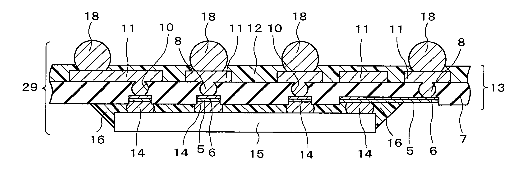
[0067] Specifically, a bump 14 is disposed on each etching barrier layer 5 of the wiring board 13, and the etching barrier layer 5 of the wiring board 13 and an electrode (not shown in the drawing) provided to the semiconductor device 15 are connected to each other via this bump 14. An underfill 16 is filled around the bump 14 in the space between the wiring board 13 and the semiconductor device 15. A solder ball 18 is disposed on the exposed portion, specifically, on a portion of the pad electrode, of the upper-layer wiring 11 of the wiring board 13. This solder ball 18 is connected to an electrode of the semiconductor device 15 via the upper-layer wiring 11, the internal conductor 8 formed inside the via hole 10, the lower-layer wiring composed of the wiring body 6 and the etching barrier layer 5, and the bump 14. This semiconductor package 29 is mounted to a mounting board (not shown in the drawing) via the solder ball 18. In the semiconductor package 29 of the present modificati...


PUM


Abstract

A wiring board in which lower-layer wiring composed of a wiring body and an etching barrier layer is formed in a concave portion formed on one face of a board-insulating film, upper-layer wiring is formed on the other face of the board-insulating film, and the upper-layer wiring and the wiring body of the lower-layer wiring are connected to each other through a via hole formed in the board-insulating film. The via hole is barrel-shaped, bell-shaped, or bellows-shaped.

Description

BACKGROUND OF THE INVENTION [0001] 1. Field of the Invention [0002] The present invention relates to a wiring board on which semiconductor devices and various other types of devices are mounted, to a method for manufacturing the same, and to a semiconductor package that uses the wiring board. [0003] 2. Description of the Related Art [0004] Due to recent advances in the performance and functionality of semiconductor devices, the number of terminals is increasing, the terminals are being spaced apart at a narrower pitch, and processing speed is also increasing. This has led to increased demand for higher-density wiring and higher speed in wiring boards for packaging on which a semiconductor device is mounted. A built-up printed board that is a type of multilayer wiring board is an example of the conventional wiring board for packaging that is commonly used. [0005]FIG. 1 is a sectional view showing the conventional built-up printed board in general use. In the conventional built-up pri...

Claims


Application Information

Patent Timeline
Patent Type & Authority Applications(United States)
IPC IPC(8): H05K1/11H05K1/03
CPCH01L21/486H01L21/6835H01L23/49811H01L23/49822H01L23/49827H01L24/32H01L25/0657H01L2221/68345H01L2224/16225H01L2224/32057H01L2224/32225H01L2224/48227H01L2224/73265H01L2224/83385H01L2224/92125H01L2225/06517H01L2225/06524H01L2225/06541H01L2225/06572H01L2225/06586H01L2924/01013H01L2924/01029H01L2924/01046H01L2924/01078H01L2924/01079H01L2924/09701H01L2924/14H01L2924/15311H01L2924/1532H01L2924/30107H01L2924/3011H05K3/0055H05K3/20H05K3/421H05K3/4644H05K2201/09563H05K2201/09863H05K2203/0796H01L24/48H01L2924/01005H01L2924/01006H01L2924/01019H01L2924/01033H01L2924/014H01L2224/73204H01L24/73H01L2924/10253H01L2924/12041H01L2224/16235H01L2924/00H01L2924/00012H01L2924/00011H01L2924/00014H01L2924/15183H01L2924/351H01L2224/0401H01L2224/45099H01L2224/45015H01L2924/207
Inventor YAMAMICHI, SHINTAROKIKUCHI, KATSUMIMURAI, HIDEYAFUNAYA, TAKUOMAEDA, TAKEHIKOOGAWA, KENTATSUKANO, JUNHONDA, HIROKAZU
Owner RENESAS ELECTRONICS CORP
Why Eureka
Try Eureka