Method for manufacturing display device and display device manufacturing apparatus

a display device and manufacturing method technology, applied in the direction of identification means, instruments, cleaning using liquids, etc., can solve the problems of display performance not being uniform, quality problems of display devices, etc., and achieve the effect of lowering display quality

Inactive Publication Date: 2005-02-17
PANASONIC LIQUID CRYSTAL DISPLAY CO LTD +1
View PDF6 Cites 11 Cited by
  • Summary
  • Abstract
  • Description
  • Claims
  • Application Information

AI Technical Summary

Benefits of technology

[0017] In the case when the thin film formed on the glass substrate is treated with use of the solution containing chemicals as described above, the “roller marks” can be kept from forming, by supplying the chemical solution around the supporting member coming into contact with the back of the glass substrate. This enables production of display devices making use of glass sheets as substrates, such as liquid-crystal display devices and self-luminous display devices, without any lowering of the display quality that is a typical characteristic the display devices must have.

Problems solved by technology

If a display device is set up thereon in such a state, the steps in the substrate may cause the scattering of light to cause a defect that the display performance comes non-uniform that is one of important characteristics required as display devices.
However, according to the results of experiments made by the present inventors, even when the solution is supplied also to the back side of the glass substrate, etching non-uniformity called “roller marks” is formed at positions where the back of the glass substrate comes into contact with glass-substrate-supporting members, e.g., transport rollers, to cause a problem on quality as display devices.

Method used


Image

  • Method for manufacturing display device and display device manufacturing apparatus
  • Method for manufacturing display device and display device manufacturing apparatus
  • Method for manufacturing display device and display device manufacturing apparatus

Examples


example 1

[0051]FIGS. 6A to 6D schematically illustrate the steps of manufacturing a polycrystalline TFT (thin-film transistor) used in liquid-crystal display devices. FIG. 11 is a flow chart of its manufacturing steps.

[0052] First, as shown in FIG. 6A, on a glass substrate 1 having been cleaned in a cleaning step (S120), an amorphous silicon film 10a (layer thickness: 10 to 100 nm) is formed by a well known process CVD (chemical vapor deposition) (S121). Thereafter, the amorphous silicon film 10a is cleaned (S122)

[0053] This amorphous silicon film 10a is crystallized by means of an excimer laser or the like to form a polycrystalline silicon film 10b (S123), and the substrate is cleaned (S124).

[0054] Next, as shown in FIG. 6B, the polycrystalline silicon film 10b is worked in a predetermined size, and thereafter, on this polycrystalline silicon film 10b, a gate insulation film 11 (silicon oxide film of about 100 nm in layer thickness) is formed by a well known process, e.g., plasma TEOS (T...

example 2

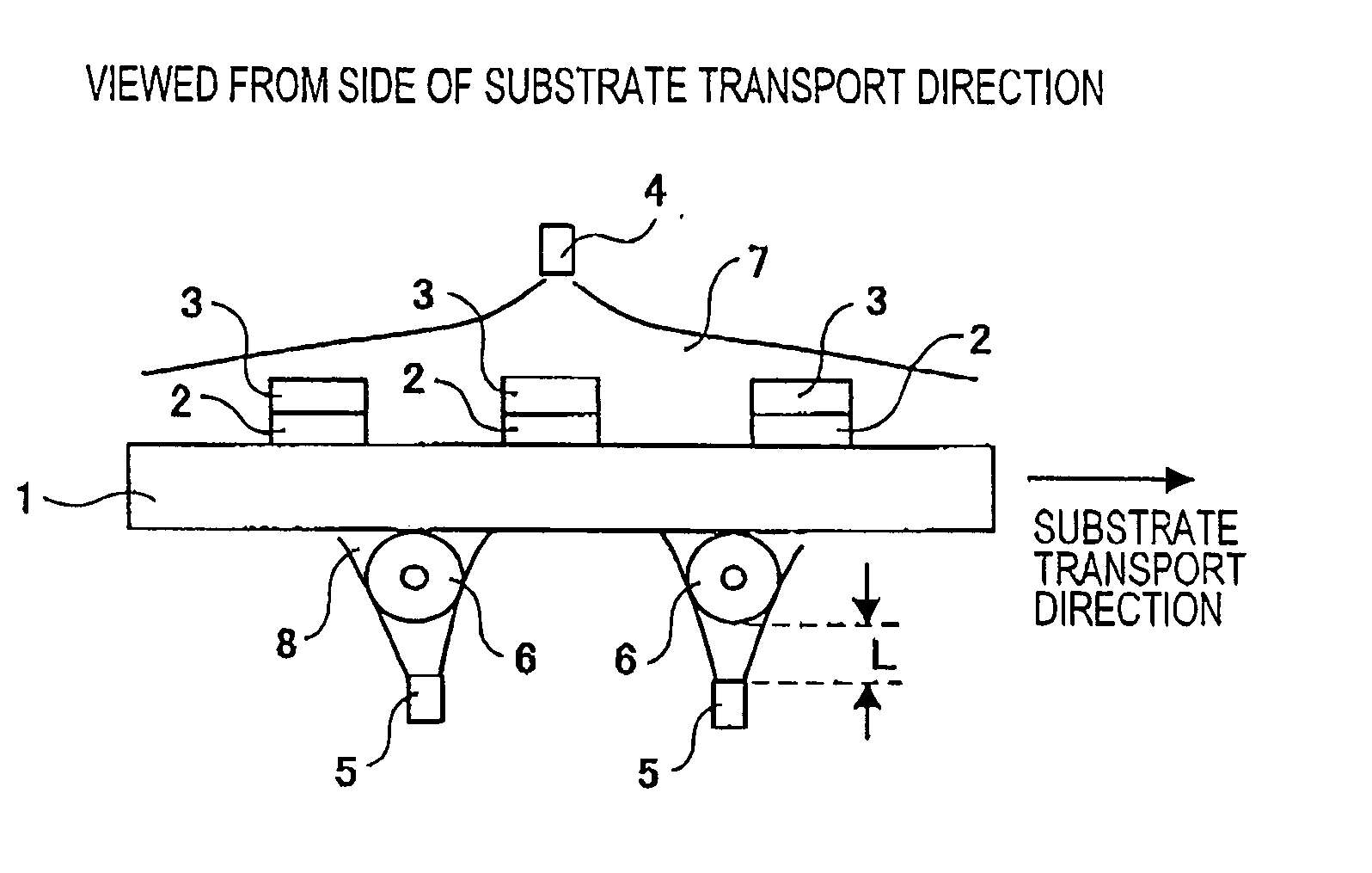
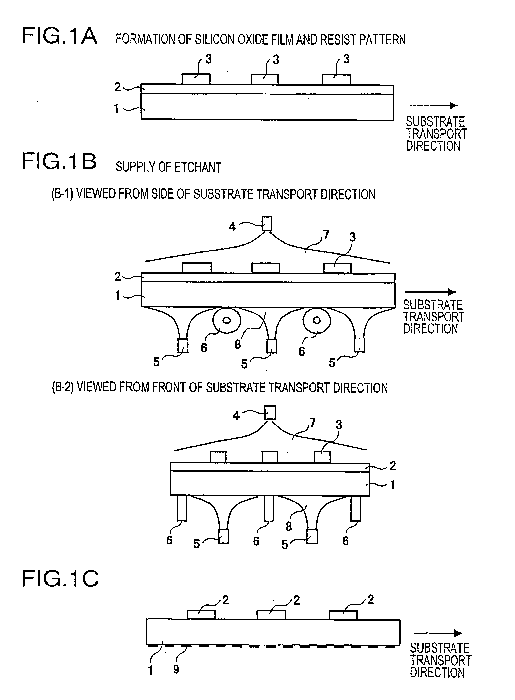
[0066] The glass substrate used in etching, the thin film to be treated, the etching apparatus and the etching conditions are the same as those in Example 1. What differs from Example 1 is the method of supplying the second solution, and the method shown in FIGS. 4A and 4B is used in this Example 2.

[0067] That is, as shown in FIG. 12, in the step of forming contact holes (S132′), in order to immediately remove the insoluble residues having adhered to the back of the glass substrate 1, the apparatus is so set that the second solution is supplied through nozzles so disposed that the second solution 8 is jetted to regions where the supporting members 6 and the back (the side on which no thin film is formed) of the glass substrate 1 come into contact, and in the direction opposite to the glass substrate 1 transport direction (the direction shown by an arrow A in FIG. 4A).

[0068] Results of the foregoing are shown together in item (2) in Table 1. Like the case of Example 1, it was able ...

example 3

[0069] The glass substrate used in etching, the thin film to be treated, the etching apparatus and the etching conditions are the same as those in Example 1. What differs from Example 1 is the method of supplying the second solution, and the method shown in FIGS. 5A and 5B are used in this Example 3. That is, the nozzles 5, which are positioned below the supporting members 6, are disposed between supporting members 6 adjacent to one another in the direction of transport of the glass substrate 1. Then, as shown in FIG. 12, in the step of forming contact holes (S132′), the apparatus is so set that the second solution jetted from the nozzles 5 is supplied to regions where adjacent supporting members 6 each come into contact with the back of the glass substrate 1. The position of each nozzle 5 disposed between adjacent two supporting members 6 (the distance between the nozzle and each supporting member is 5 to 100 mm) may preferably be the middle of the two supporting members.

[0070] Re...


PUM

PropertyMeasurementUnit
distanceaaaaaaaaaa
sizeaaaaaaaaaa
widthaaaaaaaaaa

Abstract

Where a thin film formed on a glass substrate is etched with a solution containing a fluoride, insoluble residues formed by the reaction of the solution with glass substrate components adhere to the back of the substrate to cause etching non-uniformity called roller marks. So, a solution is supplied directly to supporting member for supporting the glass substrate, or concentratedly to region where the substrate and the supporting member come into contact and from a position opposite to the transporting direction of the substrate, or to both the supporting members and regions where the substrate and the supporting members come into contact. This enables the roller marks to be kept from forming, consequently making it possible to improve display quality of display devices.

Description

BACKGROUND OF THE INVENTION [0001] This invention is concerned with treatment for etching or cleaning a thin film formed on a platelike glass substrate for use in flat-panel display, and more particularly relates to a method for manufacturing a display device in which marks of rollers for supporting and transporting glass substrate have been kept from forming on the back of the glass substrate, and an apparatus for manufacturing such a display device. [0002] In general, in methods for manufacturing liquid-crystal display devices, an etching step of processing into stated shapes semiconductor films such as thin films formed on glass substrates, as exemplified by an amorphous silicon film, a polycrystalline silicon film and also a silicon oxide film, is the step of etching and removing the thin film by means of a solution, using as a mask a resist film formed on the thin film. A cleaning step is also the step of applying a solution to the thin film to remove foreign matters and contam...

Claims


Application Information

Patent Timeline
Patent Type & Authority Applications(United States)
IPC IPC(8): B08B3/02B08B3/08G02F1/13G02F1/1333G09F9/00H01L21/00H01L21/306H01L21/311H01L21/336H01L51/00H01L51/40H01L51/50H05B33/02H05B33/10
CPCH01L21/31111H01L21/67028H01L51/0019H01L29/66765H01L29/66757H10K71/236F16D48/02F16D25/088F16D2048/0218
Inventor OHSAWA, TOSHIYUKITAKAHARA, YOICHIKANEKO, TOSHIKISONODA, DAISUKE
Owner PANASONIC LIQUID CRYSTAL DISPLAY CO LTD
Why Eureka
Try Eureka