

Semiconductor light emitting device and method for manufacturing same
- Summary
- Abstract
- Description
- Claims
- Application Information
AI Technical Summary
Benefits of technology
Problems solved by technology
Method used
Image

Examples
first preferred embodiment
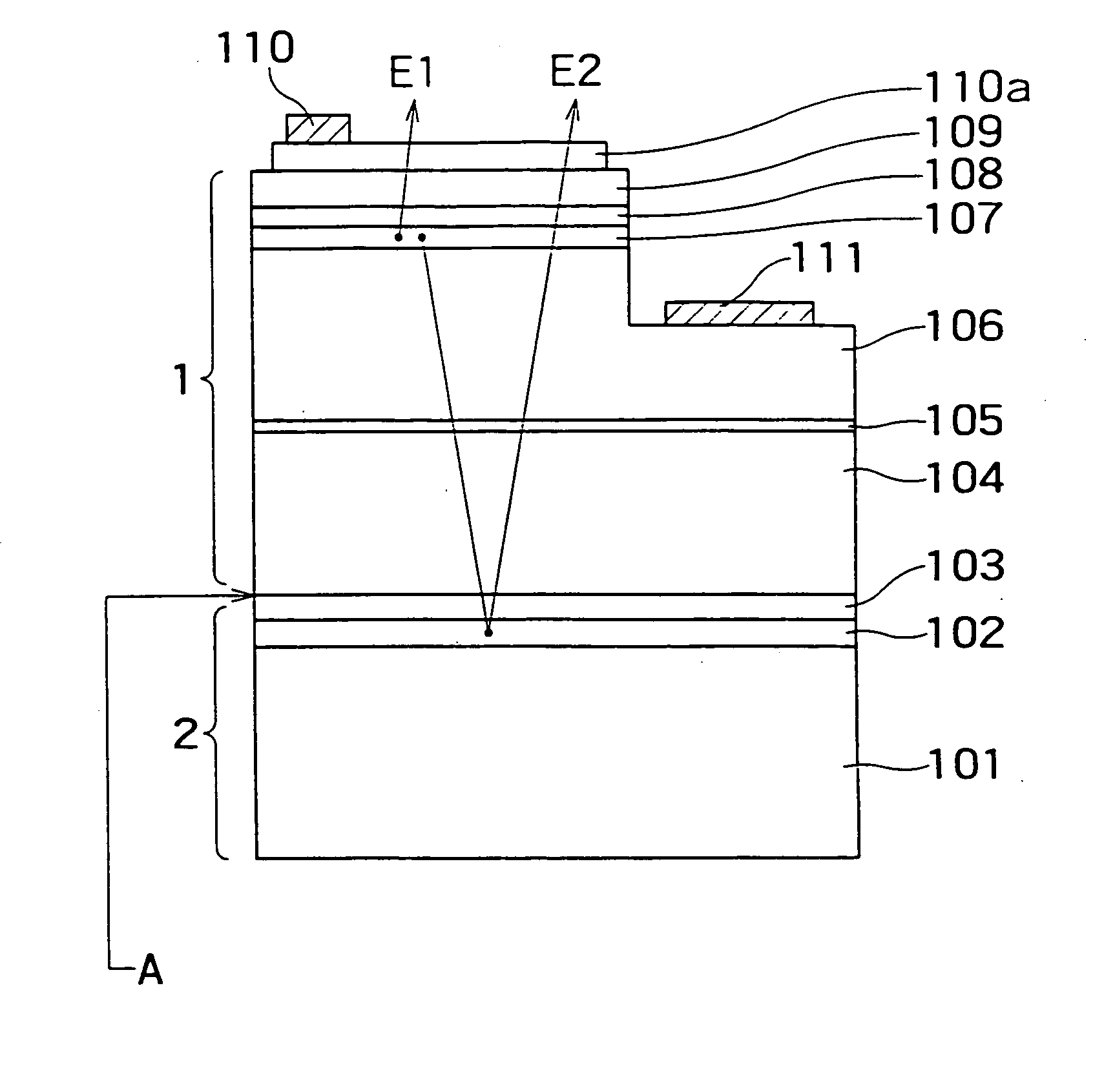
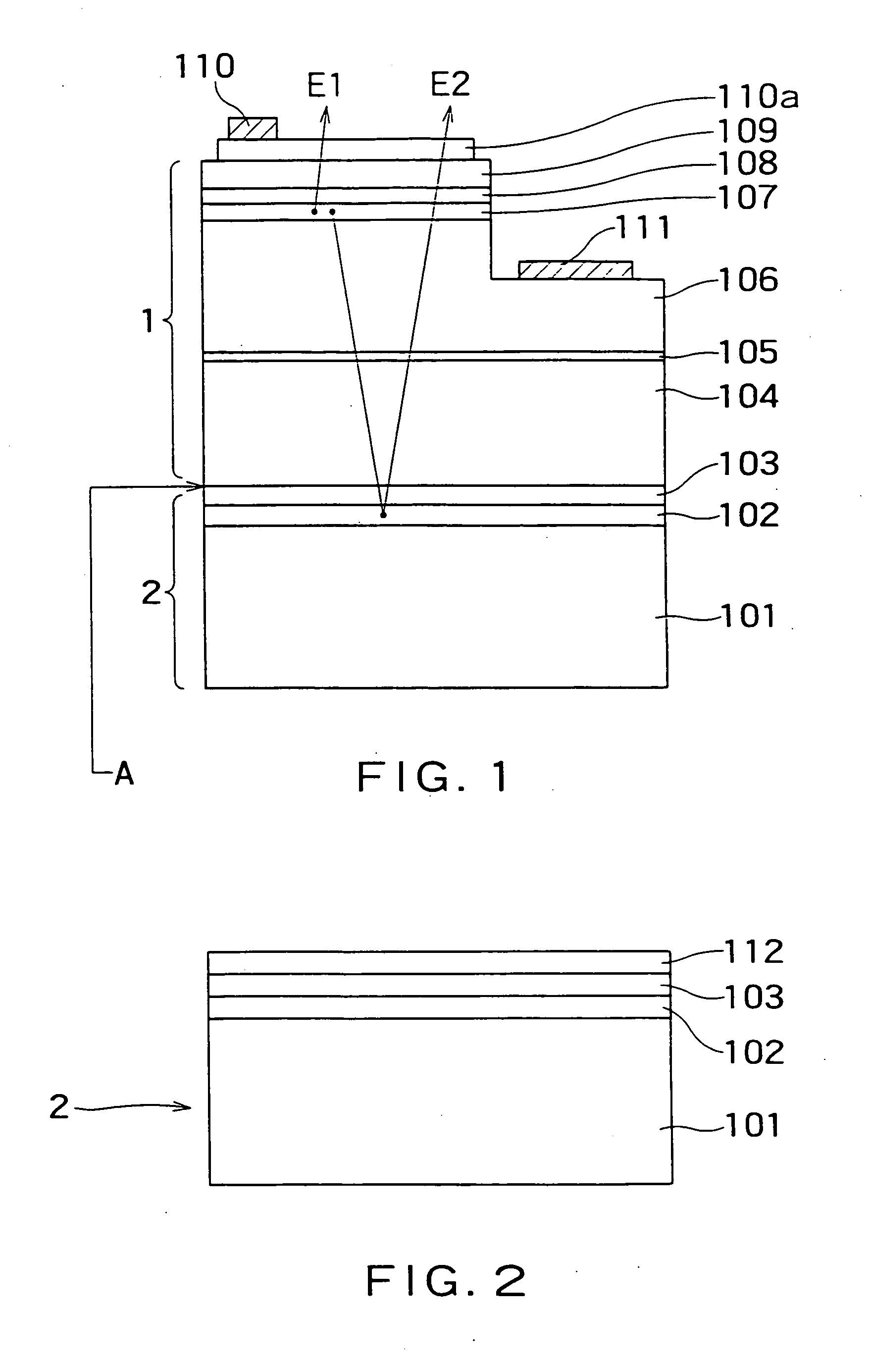
[0052]FIG. 1 is a schematic sectional view showing the first preferred embodiment of a semiconductor white light emitting device according to the present invention. A semiconductor light emitting element 1 for emitting blue light E1 by current injection and a semiconductor laminate 2 excited by the blue light E1 for emitting yellow light E2 are bonded to each other at a bonding surface A to constitute a semiconductor white light emitting device. As can be seen from FIG. 1, these light beams are emitted from the top side in the figure.
[0053] First, the semiconductor light emitting element 1 will be described. On the top face of a sapphire substrate 104 in the figure, there are sequentially formed a buffer layer 105, an n-type GaN cladding layer (n-type contact layer) 106, an active layer 107 having a GaN / InGaN multi-quantum well structure (MQW structure), a p-type AlGaN cladding layer 108 and a p-type GaN contact layer 109. Furthermore, the “n-type GaN cladding layer 106” will somet...
second preferred embodiment
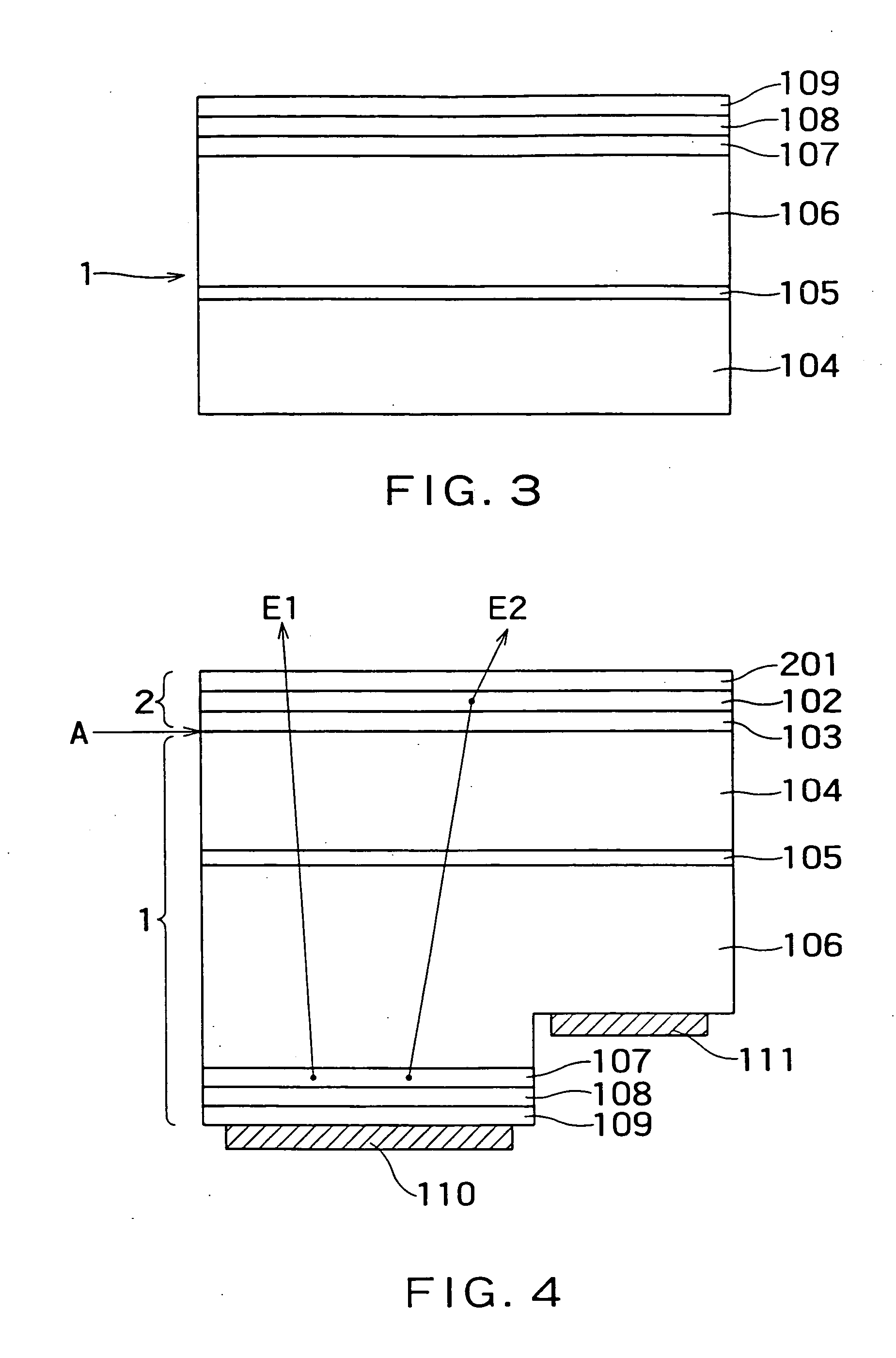
[0071] As can be seen from FIG. 4, one of different points of a semiconductor white light emitting device in the second preferred embodiment from the device in the first preferred embodiment (FIG. 1) is that the substrate 104 side of a semiconductor light emitting element 1 serves as a light emitting surface and that a semiconductor laminate 2 is bonded to the side of the light emitting surface.
[0072]FIG. 4 is a schematic sectional view showing the second preferred embodiment of a semiconductor white light emitting device according to the present invention. The same reference numbers are given to elements corresponding to those in the first preferred embodiment (FIG. 1). As in the case with the first preferred embodiment (FIG. 1), a semiconductor light emitting element 1 for emitting blue light E1 from an active layer 107 by current injection and a semiconductor laminate 2 excited by the blue light E1 for emitting yellow light E2 from a light emitting layer 102 are bonded to each o...
third preferred embodiment
[0078] As can be seen from FIG. 5, one of different points of a semiconductor white light emitting device in the third preferred embodiment from the device in the second preferred embodiment (FIG. 4) is that two light emitting layers 302 and 304 are formed in a semiconductor laminate 2.
[0079]FIG. 5 is a schematic sectional view showing the third preferred embodiment of a semiconductor white light emitting device according to the present invention. The same reference numbers are given to elements corresponding to those in the second preferred embodiment (FIG. 4). A semiconductor light emitting element 1 for emitting blue light E1 from an active layer 107 by current injection and a semiconductor laminate 2, which is excited by the blue light E1 for emitting green light E2 from a first light emitting layer 304 and which is excited by the green light E2 and the blue light E1 for emitting red light E3 from a second light emitting layer 302, constitute a semiconductor white light emittin...
PUM
 Abstract
Description
Claims
Application Information