Plasma display panel
a technology of display panel and plasma, which is applied in the direction of gas discharge electrode, sustain/scan electrode, gas discharge tube, etc., can solve the problems of difficult brightness, unstable writing operation, and decrease the time for the sustain period, so as to reduce the discharge voltage generated by the third electrode, stable address characteristics, and reduce the discharge time lag
- Summary
- Abstract
- Description
- Claims
- Application Information
AI Technical Summary
Benefits of technology
Problems solved by technology
Method used
Image
Examples
embodiment 1
[0044] [Embodiment 1]
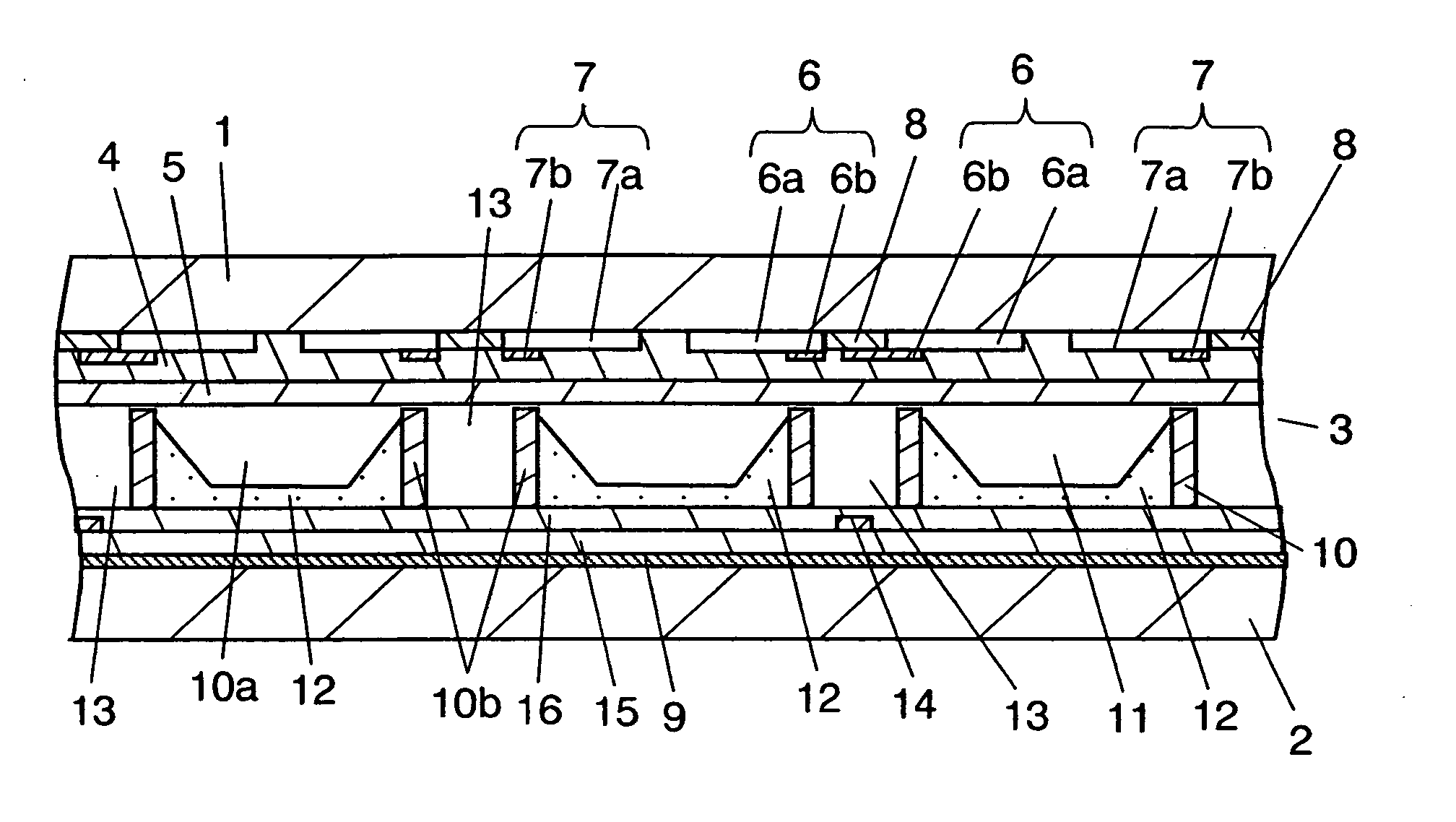
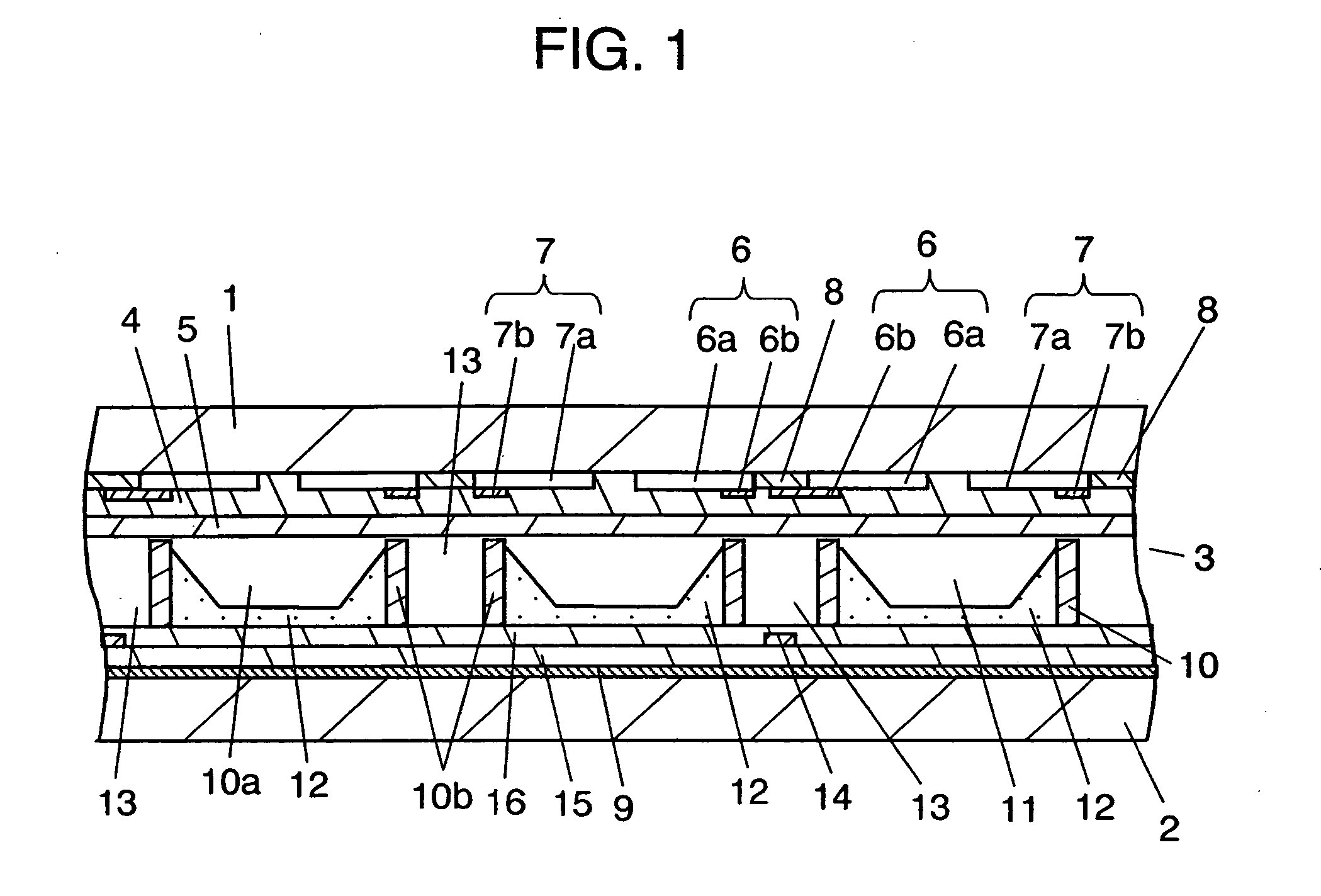
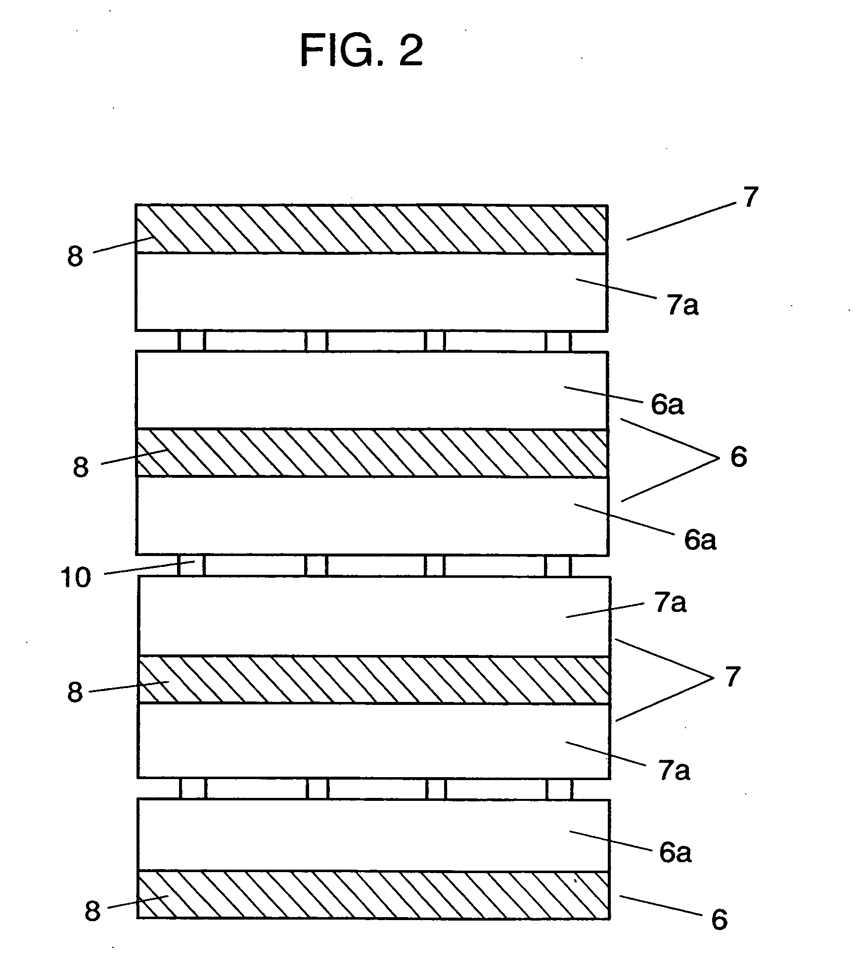
[0045]FIG. 1 is a cross sectional view showing the plasma display panel according to the embodiment 1 of the invention, FIG. 2 is a plan view schematically showing the array of electrodes on the front substrate that is the first substrate, FIG. 3 is a perspective view schematically showing the rear substrate that is the second substrate, and FIG. 4 is a plan view of the rear substrate that is the second substrate. Further, FIG. 5, FIG. 6, and FIG. 7 are cross sectional views respectively cut off along the A-A line, the B-B line, and the C-C line of FIG. 4.
[0046] As shown in FIG. 1, a front substrate 1 made of glass that is the first substrate and a rear substrate 2 made of glass that is the second substrate are arranged facing each other with a discharge space 3 between them, and as a gas which radiates ultraviolet light when a discharge is applied, neon, xenon, or a mixture of them is charged in the discharge space 3. On the front substrate 1, an electrode gro...
embodiment 2
[0072] [Embodiment 2]
[0073]FIG. 13 is a plan view showing the structure of an important portion of the plasma display panel according to the embodiment 2 of the invention. In the embodiment 2, a discharge area for inducing a priming discharge between the front substrate 1 and the rear substrate 2 within the interstice portion 13 is provided in the peripheral portion around the display area of the plasma display panel.
[0074] It is necessary to produce a priming discharge which itself is stable and without discharge time lag in a method for improving the addressing characteristics by such priming discharge. In the embodiment 2, a discharge area for producing an auxiliary discharge which can be a stable priming discharge is formed in the peripheral portion of the panel.
[0075] As illustrated in FIG. 13, the metal bus line 6b of the scan electrode 6 corresponding to the priming electrode 14 extends to the peripheral area around the display area 50 formed by the barrier rib 10 and simil...
embodiment 3
[0076] [Embodiment 3]
[0077]FIG. 14 is a cross sectional view showing the plasma display panel according to the embodiment 3 of the invention. In the embodiment 3, in addition to the priming electrode 14 formed on the rear substrate 2, a priming electrode 18 is formed in the area corresponding to the interstice portion 13, between the interstice portion 13 and the front substrate 1. A new voltage waveform other than that of the scan electrode 6 may be applied to this priming electrode 18, even if its potential is the same as that of the scan electrode 6. It is possible to produce a priming discharge within the interstice portion 13 at a higher speed by forming this electrode structure, hence enabling faster writing.
PUM
 Abstract
Description
Claims
Application Information


