
Switched-capacitor amplifier and analog interface circuit for charge coupled element adopting the same

a technology of switching capacitors and analog interfaces, applied in the direction of charge amplifiers, amplifiers using switched capacitors, instruments, etc., can solve the problems of more obvious variations in amplification factors with variations in processes, and become more liable to be affected by process variations, so as to reduce the capacitor ratio

Inactive Publication Date: 2005-02-24
SHARP KK
View PDF4 Cites 11 Cited by
  • Summary
  • Abstract
  • Description
  • Claims
  • Application Information

AI Technical Summary

Benefits of technology

The present invention provides a switched capacitor amplifier that can reduce the capacitor ratio even when setting the laser gain. This is achieved by using a control means that stores charges according to an input signal and changes the potential of the capacitors in opposite directions to maintain the charges at the first connection point. The control means can vary the potential of the second terminals of the capacitors while maintaining the charges at the first connection point. This allows for a higher gain without being affected by variations in manufacturing processes. The switched capacitor amplifier can also have a plurality of input signals and a pair of capacitors to output a product-sum operation of the input signals. The control means can also change the potential of the third capacitor to control the potential of the connection point. These features make the switched capacitor amplifier more efficient and faster than conventional amplifiers.

Problems solved by technology

However, the foregoing conventional structure has a problem in that when a larger gain is set, variations in amplification factor with variations in processes become more obvious.
As a result, for the larger gain, an area occupied by one capacitor becomes larger than an area occupied by the other capacitor, and it becomes more liable to be affected by variations in processes.

Method used


Image

  • Switched-capacitor amplifier and analog interface circuit for charge coupled element adopting the same
  • Switched-capacitor amplifier and analog interface circuit for charge coupled element adopting the same
  • Switched-capacitor amplifier and analog interface circuit for charge coupled element adopting the same

Examples


embodiment 1

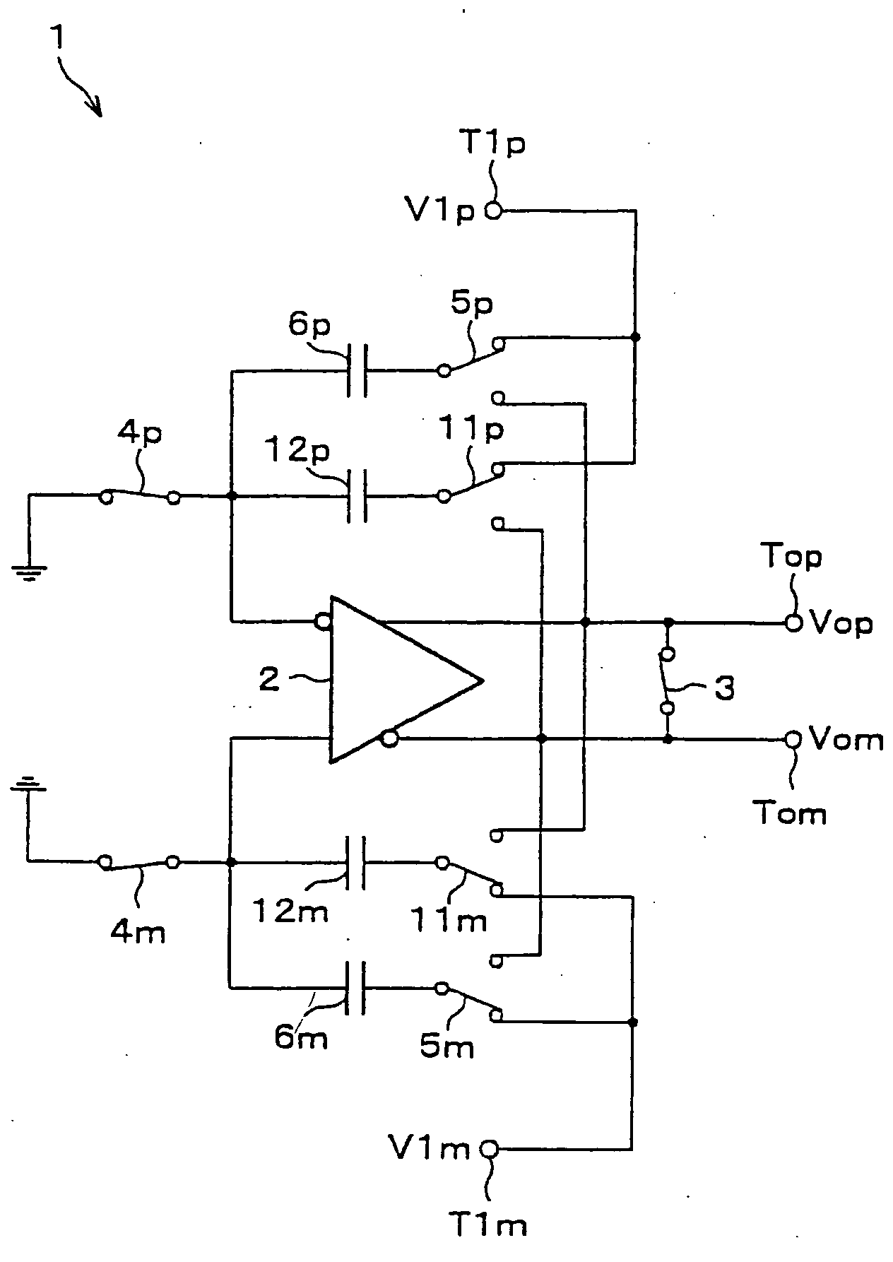
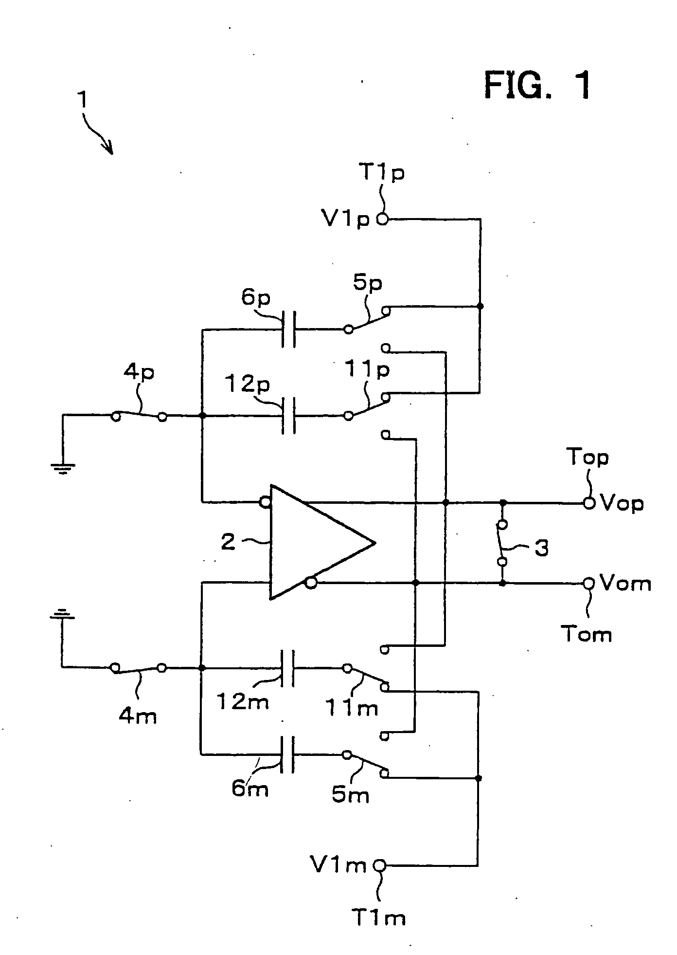
The following descriptions will explain one embodiment of the present invention in reference to FIG. 1.

A switched capacitor amplifier circuit (switched capacitor amplifier) 1 in accordance with the present invention is arranged so as to amplify with a predetermined gain, a differential input signal V1 (=V1p−V1m) as input to differential input terminals T1p and T1m serving as signal input terminals, and output the resulting signal as amplified as a differential output signal Vo(=Vop−Vom) from differential output terminals Top and Tom. The switched capacitor amplifier circuit 1 in accordance with the present embodiment is suitably applied, for example, to an analog interface of a CCD image sensor which is required to operate at high speed while suppressing adverse effects from variations in processes.

The switched capacitor amplifier circuit 1 increases an operational amplifier 2 for differential input and output. The reversing output terminal and the non-inverting output terminal...

embodiment 2

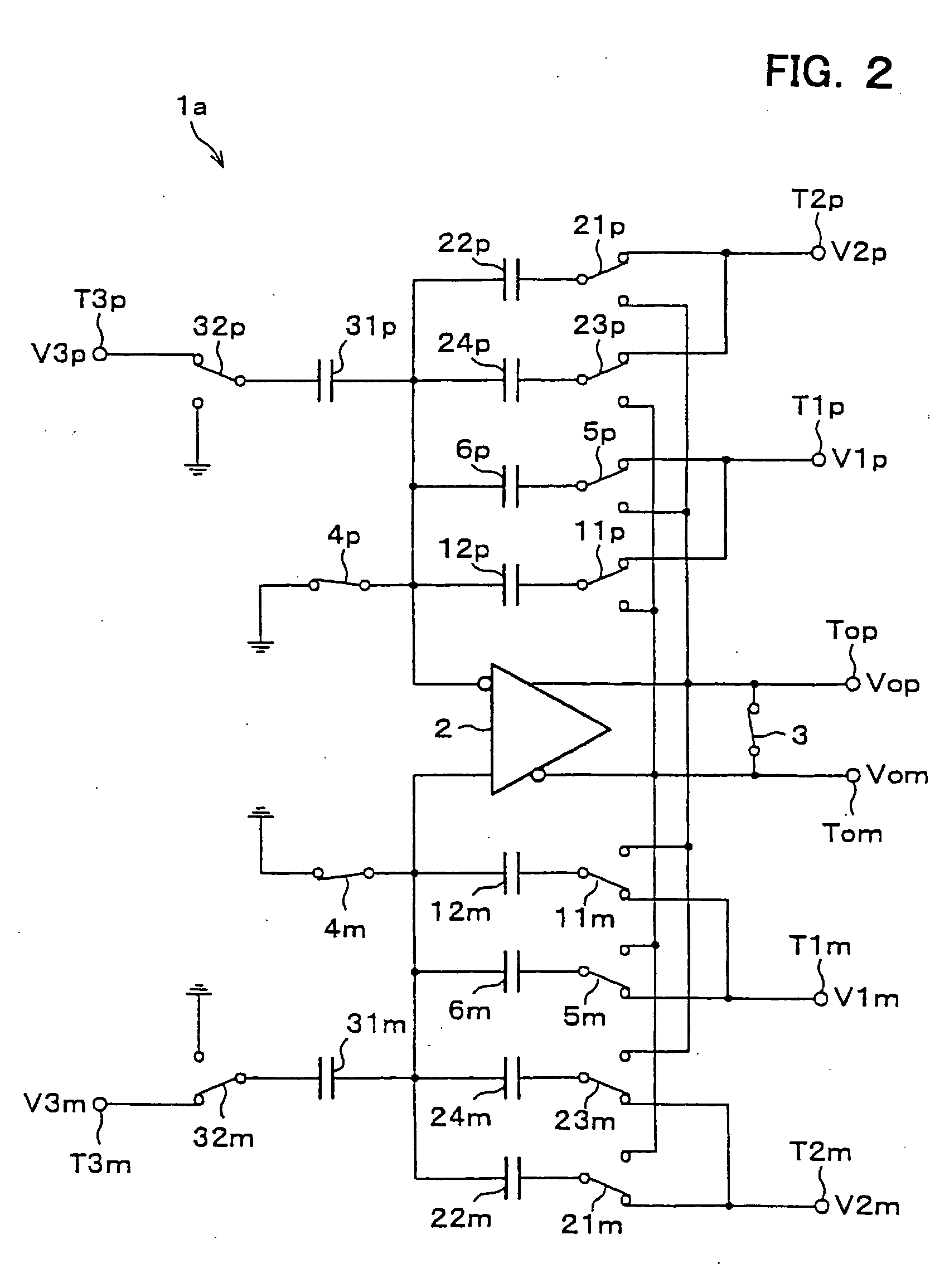
The following descriptions will explain another embodiment of the present invention in reference to FIG. 2.

In the first embodiment, explanations have been give through the case of the switched capacitor amplifier circuit 1 for amplifying a pair of differential input signals V1 (=V1p−V1m). In the present embodiment, explanations have been given through the case where a product-sum operation is performed with respect to the plural pairs (three pairs, for example) of differential input signals V1 to V3 referring to FIG. 2.

In the switched capacitor amplifier circuit 1a in accordance with the present embodiment, in addition to the structure of the switched capacitor amplifier circuit 1 shown in FIG. 1, members 21p, 22p, 23p, 24p, 21m, 22m, 23m, and 24m which are connected in the same manner as the members 5p, 6p, 11p, 12p, 5m, 6m, 11m, and 12m shown in FIG. 1. It should be noted here that these members are provided for adding and amplifying the differential input signal V2, and thus...

embodiment 3

The following descriptions will explain another embodiment of the present invention in reference to FIG. 3.

In the foregoing preferred embodiments, explanations have been given through the case of adopting a single capacitor for each of the capacitors 6p, 6m, 12p, 12m, 22p, 22m, 24p, 24m, 31p and 31m. However, the present invention is not limited to this structure, and may be realized by a plurality of capacitors connected in parallel or series, or by further connecting these plurality of capacitors connected in parallel or series a plurality of capacitors connected in parallel or series. In the foregoing preferred embodiment, explanations have been given through the case where each capacitor 6p has a fixed electrostatic capacitor value. However, the present invention is not limited to the above arrangement, and the structure with a variable electrostatic capacitor value may be adopted, and such structure may be realized by adopting a capacitor with a variable electrostatic capaci...


PUM


Abstract

In the hold phase, two negative feedback circuits constituted by the negative feedback capacitors 6p and 6m and two positive feedback circuits constituted by positive feedback capacitors are provided between an input terminal and an output terminal of an operational amplifier. Here, in a sampling phase before a hold phase, charges according an input signal V1p is stored in each of the capacitors, and charges according to an input signal V1p are stored in each of the capacitors. As a result, a gain of the switched capacitor amplifier circuit is derived from (Ca+C) / (Ca−Cx) wherein Ca indicates an electrostatic capacitance of the negative feedback capacitors, and Cx indicates an electrostatic capacitance of the positive feedback capacitors, and thus the gain can be increased without significantly increasing an electrostatic capacitance ratio.

Description

FIELD OF THE INVENTION The present invention relates to a switched capacitor amplifier, and more particularly relates to a switched capacitor amplifier which permits an increase in gain without significantly increasing an electrostatic capacitance ratio of a capacitor. BACKGROUND OF THE INVENTION Conventionally, switched capacitor amplifiers have been used in a variety of fields, for example, as a PGA (Programmable Gain Amplifier) for amplifying an analog signal as input via a CDS (Correlated Double Sampling) circuit from a CCD (Charge-Coupled Device) as disclosed in, for example, 2000 IEEE International Solid State Circuits Conference, Digest of Technical papers, pp190-191. FIG. 5 shows a switched capacitor amplifier circuit 101 as an example of generally used conventional differential input and output circuits, wherein in the sampling interface, signals Vip and Vim as input as differential input signals Vi are input to input capacitors 107p and 107m via switches 108p and 108m re...

Claims


Application Information

Patent Timeline
Patent Type & Authority Applications(United States)
IPC IPC(8): G11C27/02H03H19/00H03F3/00H03F3/45H03F3/70
CPCH03F3/005G11C27/026
Inventor FUJIMOTO, YOSHIHISA
Owner SHARP KK
Learn More