

Switched-capacitor amplifier and analog interface circuit for charge coupled element adopting the same
a technology of capacitor amplifier and analog interface circuit, which is applied in the direction of charge amplifier, pulse technique, instruments, etc., can solve the problems of more obvious variations in amplification factor with variations in processes, and becomes more liable to be affected by process variations, so as to reduce the capacitor ratio
- Summary
- Abstract
- Description
- Claims
- Application Information
AI Technical Summary
Benefits of technology
Problems solved by technology
Method used
Image

Examples
embodiment 1
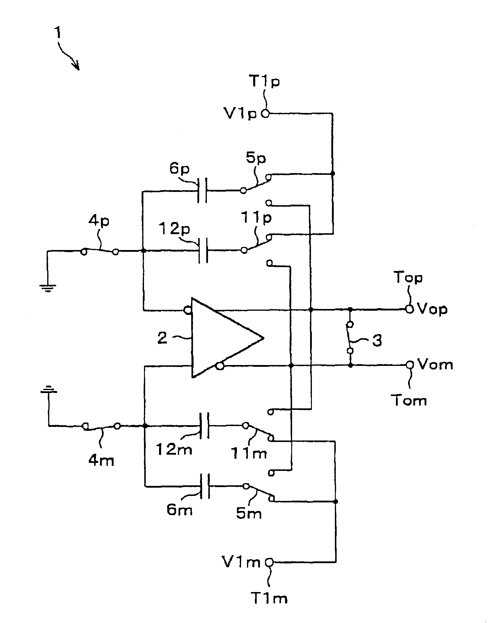
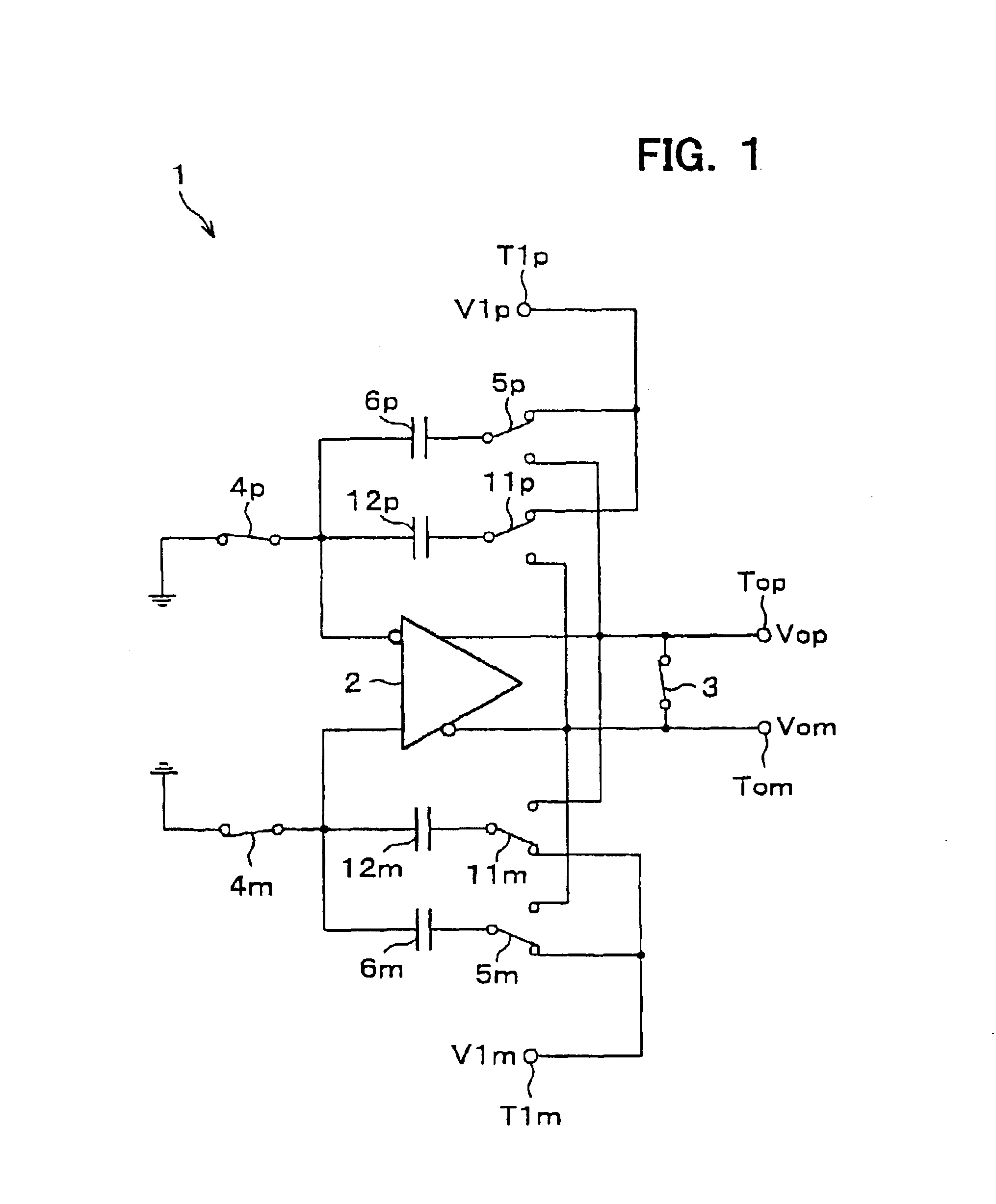
The following descriptions will explain one embodiment of the present invention in reference to FIG. 1.
A switched capacitor amplifier circuit (switched capacitor amplifier) 1 in accordance with the present invention is arranged so as to amplify with a predetermined gain, a differential input signal V1(=V1p−V1m) as input to differential input terminals T1p and T1m serving as signal input terminals, and output the resulting signal as amplified as a differential output signal Vo(=Vop−Vom) from differential output terminals Top and Tom. The switched capacitor amplifier circuit 1 in accordance with the present embodiment is suitably applied, for example, to an analog interface of a CCD image sensor which is required to operate at high speed while suppressing adverse effects from variations in processes.
The switched capacitor amplifier circuit 1 increases an operational amplifier 2 for differential input and output. The reversing output terminal and the non-inverting output terminal of th...
embodiment 2
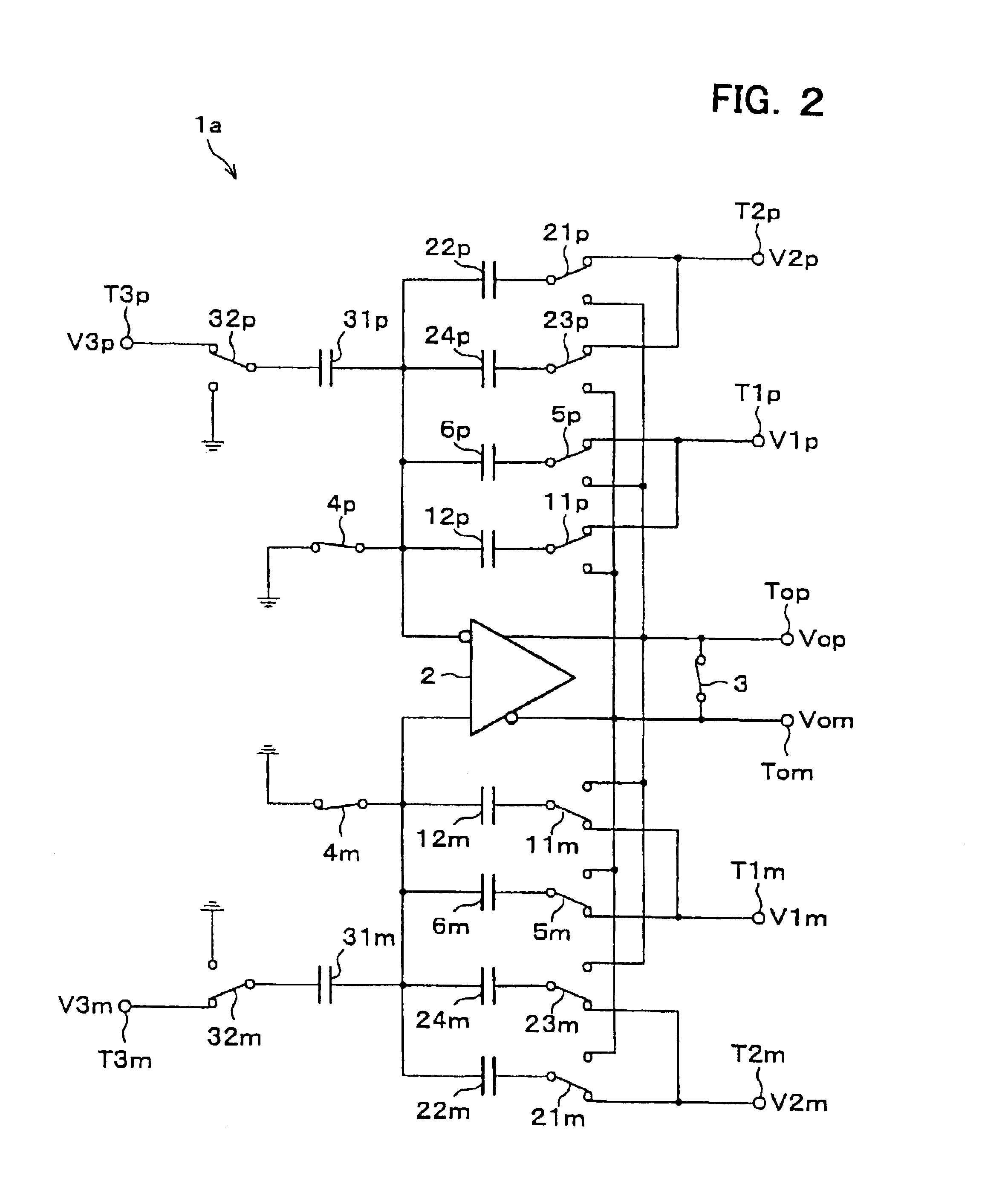
The following descriptions will explain another embodiment of the present invention in reference to FIG. 2.
In the first embodiment, explanations have been give through the case of the switched capacitor amplifier circuit 1 for amplifying a pair of differential input signals V1(=V1p−V1m). In the present embodiment, explanations have been given through the case where a product-sum operation is performed with respect to the plural pairs (three pairs, for example) of differential input signals V1 to V3 referring to FIG. 2.
In the switched capacitor amplifier circuit la in accordance with the present embodiment, in addition to the structure of the switched capacitor amplifier circuit 1 shown in FIG. 1, members 21p, 22p, 23p, 24p, 21m, 22m, 23m, and 24m which are connected in the same manner as the members 5p, 6p, 11p, 12p, 5m, 6m, 11m, and 12m shown in FIG. 1. It should be noted here that these members are provided for adding and amplifying the differential input signal V2, and thus the n...
embodiment 3
The following descriptions will explain another embodiment of the present invention in reference to FIG. 3.
In the foregoing preferred embodiments, explanations have been given through the case of adopting a single capacitor for each of the capacitors 6p, 6m, 12p, 12m, 22p, 22m, 24p, 24m, 31p and 31m. However, the present invention is not limited to this structure, and may be realized by a plurality of capacitors connected in parallel or series, or by further connecting these plurality of capacitors connected in parallel or series a plurality of capacitors connected in parallel or series. In the foregoing preferred embodiment, explanations have been given through the case where each capacitor 6p has a fixed electrostatic capacitor value. However, the present invention is not limited to the above arrangement, and the structure with a variable electrostatic capacitor value may be adopted, and such structure may be realized by adopting a capacitor with a variable electrostatic capacitor...
PUM
 Abstract
Description
Claims
Application Information