Apparatus and method for measuring each thickness of a multilayer stacked on a substrate

a multi-layer, substrate technology, applied in the direction of optical radiation measurement, semiconductor/solid-state device testing/measurement, instruments, etc., can solve the problems of inaccurate measurement thickness, high cost of monitoring process, and inability to measure thickness accurately

Inactive Publication Date: 2005-02-24
SAMSUNG ELECTRONICS CO LTD
View PDF6 Cites 14 Cited by
  • Summary
  • Abstract
  • Description
  • Claims
  • Application Information

AI Technical Summary

Benefits of technology

[0038] According to the present invention, even though an actual stack structure of the multilayer may vary from the originally designed structure, the thickness of the multilayer may be accurately measured and satisfy a reliability condition, by changing the recipe data.

Problems solved by technology

As a result, cost for the measuring process using the monitoring wafer is very high.
In addition, there is a problem in that the thickness of the thin layer on the monitoring wafer is not always identical to the thickness of the thin layer on the patterned wafer.
Therefore, the measuring method of the thickness of the thin layer using the patterned wafer has a fundamental problem in that the thickness of the layer needs to be measured without destroying the variable multilayer to prevent the patterned wafer from being damaged.
However, the dual beam spectrometry method has a problem in that the measured thickness is not accurate in a case where the layer is very thin or has a multilayer structure in which a plurality of layers is stacked on the wafer.
Therefore, when the information on the multilayer is not accurate, the measured spectrum may not be identical to the theoretical spectrum, and the measured thickness of the multilayer may not be reliable.
However, when a process failure is generated during formation of one of the component layers in the multilayer, and the actual stacked structure of the multilayer is different from an expected structure of the multilayer, the structural information of the multilayer may not be accurately known.
As a result, the thickness of the component layer is not accurately measured by the dual beam spectrometry method or the spectroscopic ellipsometry method.
In particular, when the multilayer is formed to have a locally different stack structure due to a poor evenness of the patterned wafer, the measured thickness of a component layer in the multilayer is completely unreliable.

Method used


Image

  • Apparatus and method for measuring each thickness of a multilayer stacked on a substrate
  • Apparatus and method for measuring each thickness of a multilayer stacked on a substrate
  • Apparatus and method for measuring each thickness of a multilayer stacked on a substrate

Examples


first embodiment

[0064] First Embodiment

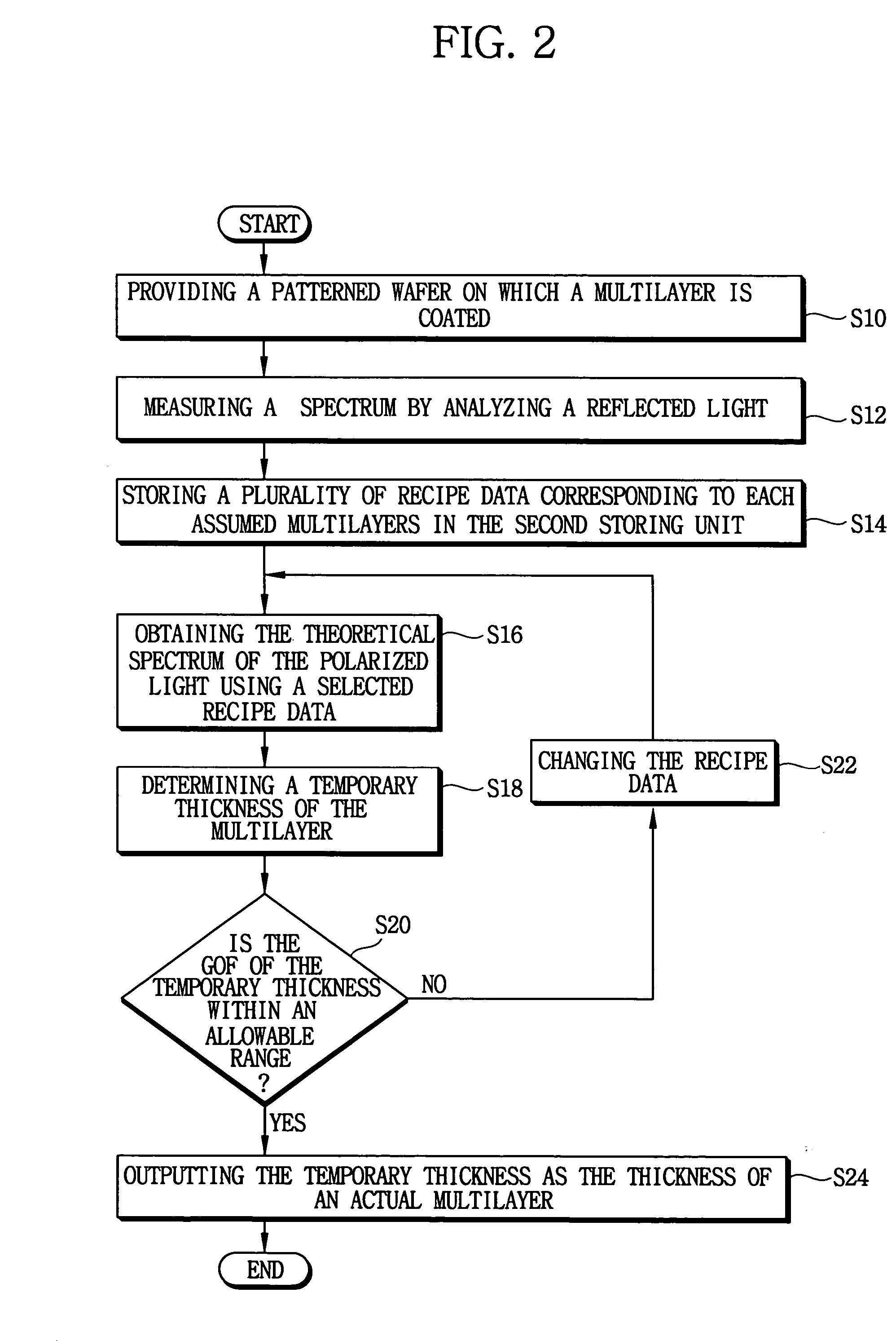
[0065]FIG. 2 is a flow chart for explaining a method of measuring a thickness of a multilayer according to a first embodiment of the present invention.

[0066] As shown in FIG. 2, in step S10, a patterned wafer on which a multilayer is coated is provided. A plurality of oxide sites (OS) is formed in a scribe line of the patterned wafer to check various process failures that may be generated during various processes. At least one of the plurality of OS has a stacked structure for measuring the thickness of the multilayer. Accordingly, the thickness of the multilayer on the patterned wafer is measured at the OS having the stacked structure.

[0067] In an exemplary embodiment, the method assumes that first through fifth layers were sequentially initially coated on an OS, and the fourth and fifth layers were sequentially etched away from the OS during an etching process. Therefore, the measuring apparatus of the present invention described above measures each thickn...

second embodiment

[0082] Second Embodiment

[0083]FIGS. 3A to 3E illustrate cross-sectional views of various hypothetical multilayers that may correspond to an actual multilayer formed on the patterned wafer.

[0084] A patterned wafer, on which a multilayer is formed, is loaded into a process chamber. In an exemplary embodiment, the multilayer on the patterned wafer is formed as follows: a first silicon nitride layer 102 having a thickness of about 260 Å, a first silicon oxide layer 104 having a thickness of about 750 Å, a second silicon nitride layer 106 having a thickness of about 500 Å, a second silicon oxide layer 108 having a thickness of about 5500 Å, a third silicon nitride layer 110 having a thickness of about 600 Å, a third silicon oxide layer 112 having a thickness of about 13,000 Å and a fourth silicon nitride layer 114 having a thickness of about 3000 Å are sequentially stacked in that order on an upper surface of a silicon wafer 100, as shown in FIG. 3A. Then, the fourth silicon nitride lay...

third embodiment

[0100] Third Embodiment

[0101] Elements and processes of a third embodiment of the present invention are substantially similar to those of the second embodiment of the present invention, except for a measuring sequence.

[0102] A patterned wafer, on which a multilayer is formed, is loaded into a process chamber. In an exemplary embodiment, the multilayer of the patterned wafer is supposed to be formed in the same process like the patterned wafer of the second embodiment described above. Specifically, the patterned wafer includes a first silicon nitride layer having a thickness of about 260 Å, a first silicon oxide layer having a thickness of about 750 Å, a second silicon nitride layer having a thickness of about 500 Å, and a second silicon oxide layer having a thickness of about 4500 Å sequentially stacked in that order from an upper surface of a substrate after an etching process.

[0103] Polarized light is directed onto a first OS, and reflected light reflected from the first OS is d...


PUM


Abstract

In an apparatus and a method of measuring a thickness of a multilayer on a substrate, a spectrum of reflected light reflected from the substrate is measured. A plurality of recipe data, each corresponding to one of a plurality of hypothetical multilayers, is stored. One of the plurality of hypothetical multilayers is initially assumed to be the multilayer actually formed on the substrate. A plurality of theoretical spectra is calculated using one of the plurality of recipe data in accordance with various theoretical thicknesses of one of the plurality of hypothetical multilayers. The measured spectrum is compared with the plurality of theoretical spectra to determine a temporary thickness of the multilayer. A reliability of the temporary thickness of the multilayer is estimated. The temporary thickness is output as a thickness of the multilayer on the substrate when the reliability of the temporary thickness is within an allowable range.

Description

BACKGROUND OF THE INVENTION [0001] 1. Field of the Invention [0002] The present invention relates to an apparatus and a method for measuring each thickness of a multilayer stacked on a substrate, e.g., a semiconductor wafer. More particularly, the present invention relates to an apparatus and method for directly measuring a thickness of the multilayer using a patterned wafer rather than a monitoring wafer. [0003] 2. Description of the Related Art [0004] Generally, a semiconductor fabricating process includes a deposition process for coating a thin layer, such as an insulation layer, a dielectric layer and a metal layer, on a wafer of monocrystalline silicon, and a photolithography process for forming a predetermined pattern on the thin layer. In addition, the thin layer is usually measured to confirm whether the thin layer is coated to a desired thickness and is etched away after performing the deposition or the photolithography processes. [0005] Conventionally, a thickness of a thi...

Claims


Application Information

Patent Timeline
Patent Type & Authority Applications(United States)
IPC IPC(8): G01B11/06H01L21/66
CPCG01B11/0641H01L22/00
Inventor HYUN, PIL-SIKKANG, SUN-JINLEE, SANG-KILJUNG, KYUNG-HO
Owner SAMSUNG ELECTRONICS CO LTD
Why Eureka
Try Eureka