Chalcogenide memory

a technology of chalcogenide and memory, applied in the field of memory devices, can solve the problems of high programming voltage and high process temperature, use of al and cu metal lines, and difficulty in making three-dimensional (3d) memory with transistors over silicon wafers

Inactive Publication Date: 2005-02-24
MACRONIX INT CO LTD
View PDF17 Cites 37 Cited by
  • Summary
  • Abstract
  • Description
  • Claims
  • Application Information

AI Technical Summary

Benefits of technology

[0005] Broadly speaking, the present invention enables the access transistor, which is also referred to as a steering element for accessing a

Problems solved by technology

However, high quality silicon is needed to fabricate transistors and this poses problems when fabricating transistors over silicon wafers.
Consequently, it is difficult to make three dimensional (3D) memory with transistors over silicon wafers.
Also, this approach requires high programming voltage and high process temperature.
High process temperatures prevent the use of Al and Cu metal lines.
For instance, the maximu

Method used


Image

  • Chalcogenide memory
  • Chalcogenide memory
  • Chalcogenide memory

Examples


Embodiment Construction

[0023] Several exemplary embodiments of the invention will now be described in detail with reference to the accompanying drawings.

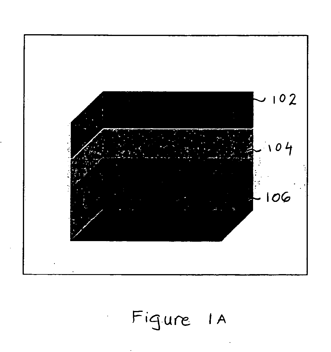
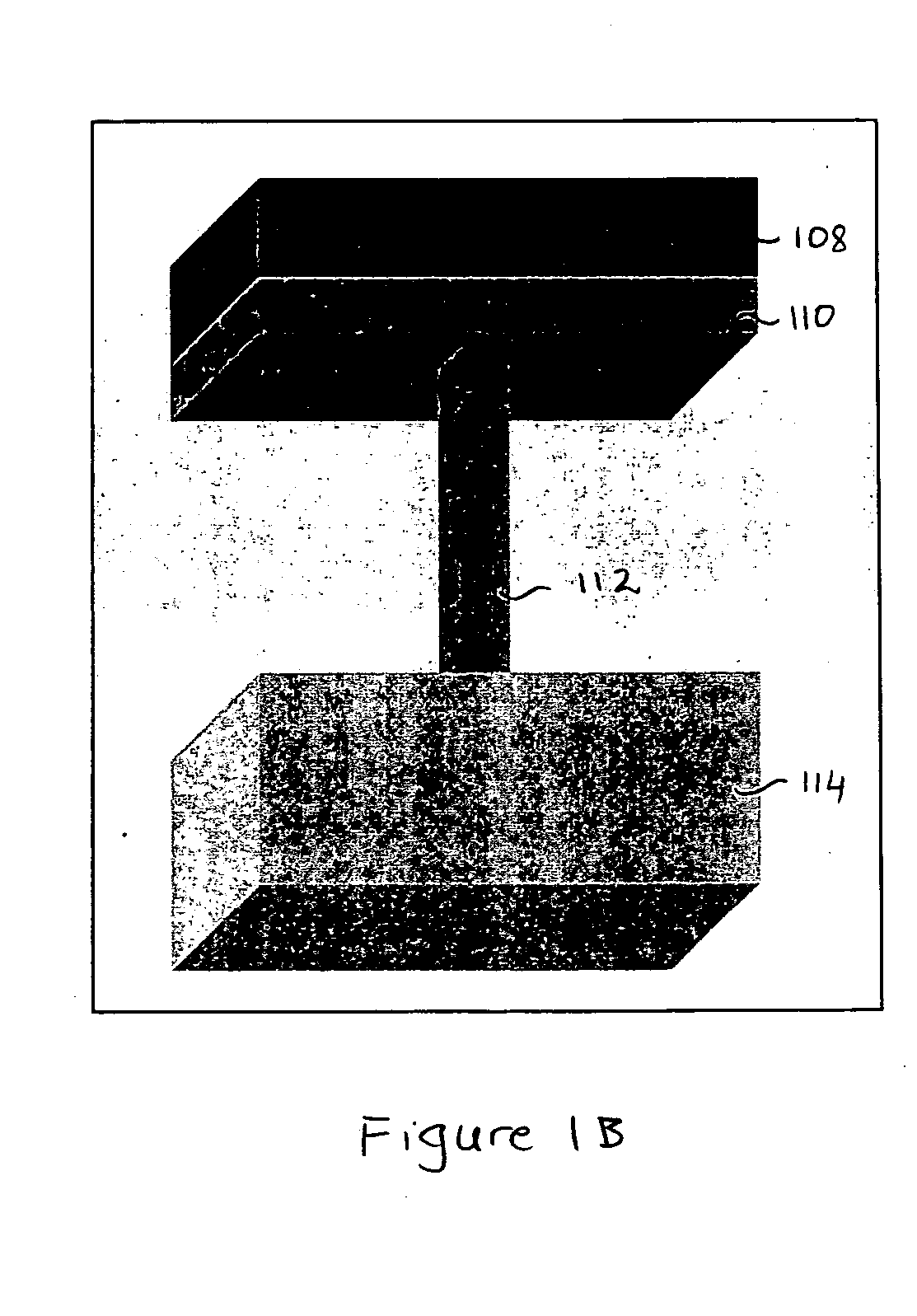
[0024] In accordance with the present invention, a threshold-switching material is incorporated into a memory cell in order to eliminate the need for access transistors. In one embodiment, the threshold-switching material is a chalcogenide material. Further information on adjusting the threshold voltage, Vth, of a material capable of changing Vth is discussed in related U.S. patent application Ser. No. 10 / 465,120.

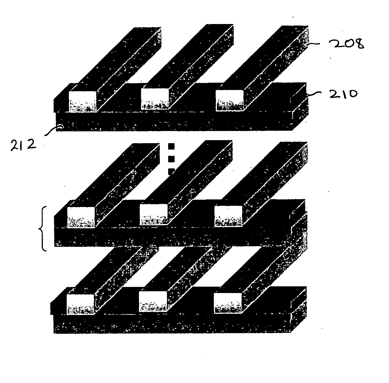
[0025] In one embodiment, the transistor-like properties of the threshold-switching material are exploited to simplify the memory cell structure by enabling the elimination of the steering element, e.g., the access transistor or P-N diode. It will be apparent to one skilled in the art that the chalcogenide memory cell may be embedded with logic circuits to form a system on a chip (SoC). Furthermore, with respect to chalcogenide, the nonvolatile...


PUM


Abstract

A memory core includes a top electrode, a bottom electrode. The memory core also includes a threshold-switching material disposed between the top electrode and the bottom electrode. The threshold-switching material serves as both a steering and a storage element. The memory cores are stacked to make the memory a 3D memory.

Description

CROSS-REFERENCE TO RELATED APPLICATIONS [0001] The present application is a continuation-in-part of a co-pending application that is commonly assigned to the assignee of the present invention, which is entitled “Transistor-Free Random Access Memory”, application Ser. No. 10 / 464,938, filed Jun. 18, 2003 (the “Parent Application”); The benefit of 35 U.S.C. Section 120 is hereby claimed with respect to the Parent Application. The present application is related to U.S. patent application Ser. No. 10 / 465,120, filed on Jun. 18, 2003 and entitled “Method for Adjusting the Threshold Voltage for a Memory Cell.” The disclosure of this related application is incorporated herein by reference for all purposes.BACKGROUND OF THE INVENTION [0002] The present invention relates generally to memory devices and, more particularly, to a memory cell structure not requiring access transistors. [0003] Typical memory cells include a steering element, e.g., one or more transistors, to access each cell. The a...

Claims


Application Information

Patent Timeline
IPC IPC(8): G11C11/00G11C13/00G11C11/34G11C16/02H01L27/10H01L27/112H01L27/24
CPCG11C13/0004G11C2213/77G11C13/0069G11C13/004
Inventor CHEN, YI CHOU
Owner MACRONIX INT CO LTD
Why Eureka
Try Eureka