Circuits and methods for characterizing random variations in device characteristics in semiconductor integrated circuits

a technology of semiconductor integrated circuits and random variations, which is applied in the direction of individual semiconductor device testing, testing circuits, instruments, etc., can solve the problems of inability to accurately measure and characterize random variations, adversely affect circuit behavior, and negligible device mismatch between neighboring devices as a result of systematic sources. , to achieve the effect of accurate measurement and characterization random variations

Active Publication Date: 2005-02-24
GLOBALFOUNDRIES US INC
View PDF10 Cites 60 Cited by
  • Summary
  • Abstract
  • Description
  • Claims
  • Application Information

AI Technical Summary

Benefits of technology

[0021] The present invention is directed to circuits and methods for measuring and characterizing random variations in device characteristics of semiconductor integrated circuit devices. More specifically, circuits and methods according to embodiments of the invention enable circuit designers to accurately measure and characterize random variations in device characteristics (such as transistor threshold voltage (Vt)) resulting from random placement of dopant atoms or line edge roughness, for purposes of integrated circuit design. Methods and circuits according to embodiments of the invention are prefe

Problems solved by technology

In contrast, random variations in device characteristics between devices of a circuit, wafer, chip or lot, are uncorrelated.
Random sources of variations, which cause device mismatch between neighboring devices in a circuit, can adversely affect circuit behavior even more drastically that systematic variations in circuits such as SRAM cells and sense amplifiers.
Indeed, since systematic sources of variation equally affect neighboring devices, device mismatch between neighboring devices as a result of systematic sources is negligible as compared to device mismatch due to random sources of device characteristic variation.
Thus, random variations in device characteristics (device mismatch) cause significantly more deviation especially in circuit performance of the above mentioned circuits, than systematic variations.
Since random variations in device characteristics are uncorrelated, methods for characterizing or modeling such random variations are difficult and inaccurate.
Although device mismatch may be caused by any number of variations in device characteristics, random variations in Vt (threshold voltage) mismatch have significant impact on circuit performance for various types of MOS circuits.
Furthermore, Vt mismatches of transistors of a sense amplifier can adversely impact the offset voltage.
In particular, because a sense amplifier senses a differential voltage applied at the gates of two neighboring sensing devices (transistors), if there is a Vt mismatch between such devices, the mismatch adds to the voltage that the sense amplifier must counter before it can amplify the desired signal.
There are various disadvantages associated w

Method used


Image

  • Circuits and methods for characterizing random variations in device characteristics in semiconductor integrated circuits
  • Circuits and methods for characterizing random variations in device characteristics in semiconductor integrated circuits
  • Circuits and methods for characterizing random variations in device characteristics in semiconductor integrated circuits

Examples


Embodiment Construction

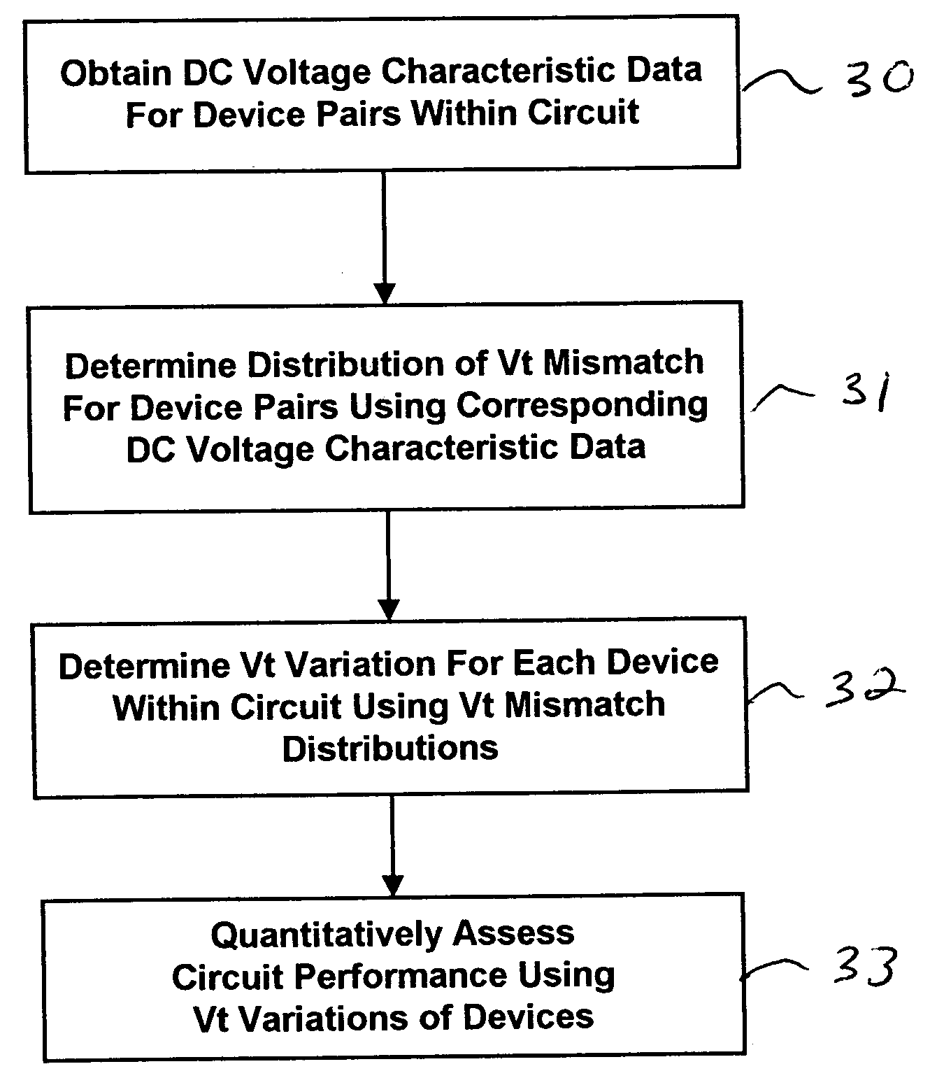
[0042] In general, circuits and methods according to embodiments of the invention are used for measuring and characterizing random variations in device characteristics of semiconductor integrated circuit devices. More specifically, circuits and methods according to embodiments of the invention enable circuit designers to accurately measure and characterized random variations in device characteristics (such as transistor threshold voltage (Vt)) resulting from random sources, for purposes of integrated circuit design. Methods and circuits according to embodiments of the invention are preferably implemented for determining variations in Vt mismatch between neighboring MOSFETs of a given circuit being analyzed / designed, such as SRAM cells or other logic devices, and using the determined variations in Vt mismatch to characterize random Vt variation of the given circuit.

[0043] In general, circuits and methods according to the present invention for characterizing device mismatch preferabl...


PUM


Abstract

Circuits and methods for measuring and characterizing random variations in device characteristics of semiconductor integrated circuit devices, which enable circuit designers to accurately measure and characterize random variations in device characteristics (such as transistor threshold voltage) between neighboring devices resulting from random sources such as dopant fluctuations and line edge roughness, for purposes of integrated circuit design and analysis. In one aspect, a method for characterizing random variations in device mismatch (e.g., threshold voltage mismatch) between a pair of device (e.g., transistors) is performed by obtaining subthreshold DC voltage characteristic data for the device pair, and then determining a distribution in voltage threshold mismatch for the device pair directly from the corresponding subthreshold DC voltage characteristic data. The voltage threshold mismatch distributions of different device pairs of a given circuit design can then be used to determine voltage threshold variations of the constituent circuit devices. The voltage threshold variation of the devices can be used to characterize the random variations of the given circuit.

Description

TECHNICAL FIELD OF THE INVENTION [0001] The present invention relates generally to circuits and methods for measuring and characterizing random variations in device characteristics in semiconductor devices. The present invention further relates to circuits and methods for measuring and characterizing device mismatch of semiconductor transistors due to local variations in device characteristics resulting from random sources, and in particular, Vt (threshold voltage) variations between neighboring MOSFETs (Metal Oxide Semiconductor Field Effect Transistors) of SRAM (Static Random Access Memory) cells or other logic devices. BACKGROUND [0002] In the design of semiconductor integrated circuits, it is very important to consider variations in device characteristics (device mismatch) such as Vt (threshold voltage) for a given circuit design, in order to achieve circuit robustness and obtain high manufacturing functional yields for such devices. [0003] In general, variations in device chara...

Claims


Application Information

Patent Timeline
IPC IPC(8): G01R27/28G01R31/26G01R31/30G01R31/317G01R31/3173G01R31/3193G11C29/50
CPCG01R31/2603G01R31/3016G01R31/31725G01R31/31727G11C2029/5002G01R31/31937G11C11/41G11C29/50G11C29/50004G01R31/3173
Inventor BHAVNAGARWALA, AZEEZFRANK, DAVID J.KOSONOCKY, STEPHEN V.
Owner GLOBALFOUNDRIES US INC
Why Eureka
Try Eureka