Ultra-thin silicon-on-insulator and strained-silicon-direct-on-insulator with hybrid crystal orientations

Active Publication Date: 2005-03-03
GLOBALFOUNDRIES US INC
View PDF7 Cites 44 Cited by
  • Summary
  • Abstract
  • Description
  • Claims
  • Application Information

AI Technical Summary

Benefits of technology

[0007] One object of the present invention is to provide a method of fabricating integrated semiconductor devices such that different types of CM

Problems solved by technology

To compensate for this discrepancy, pFETs are typically designed with larger widths in order to balance pull-up currents against the nFET pull-down currents and achieve uniform circuit switching. pFETs having larger widths are undesirable since they take up a significant amount of chip area.
Unfortun

Method used


Image

  • Ultra-thin silicon-on-insulator and strained-silicon-direct-on-insulator with hybrid crystal orientations
  • Ultra-thin silicon-on-insulator and strained-silicon-direct-on-insulator with hybrid crystal orientations
  • Ultra-thin silicon-on-insulator and strained-silicon-direct-on-insulator with hybrid crystal orientations

Examples


Embodiment Construction

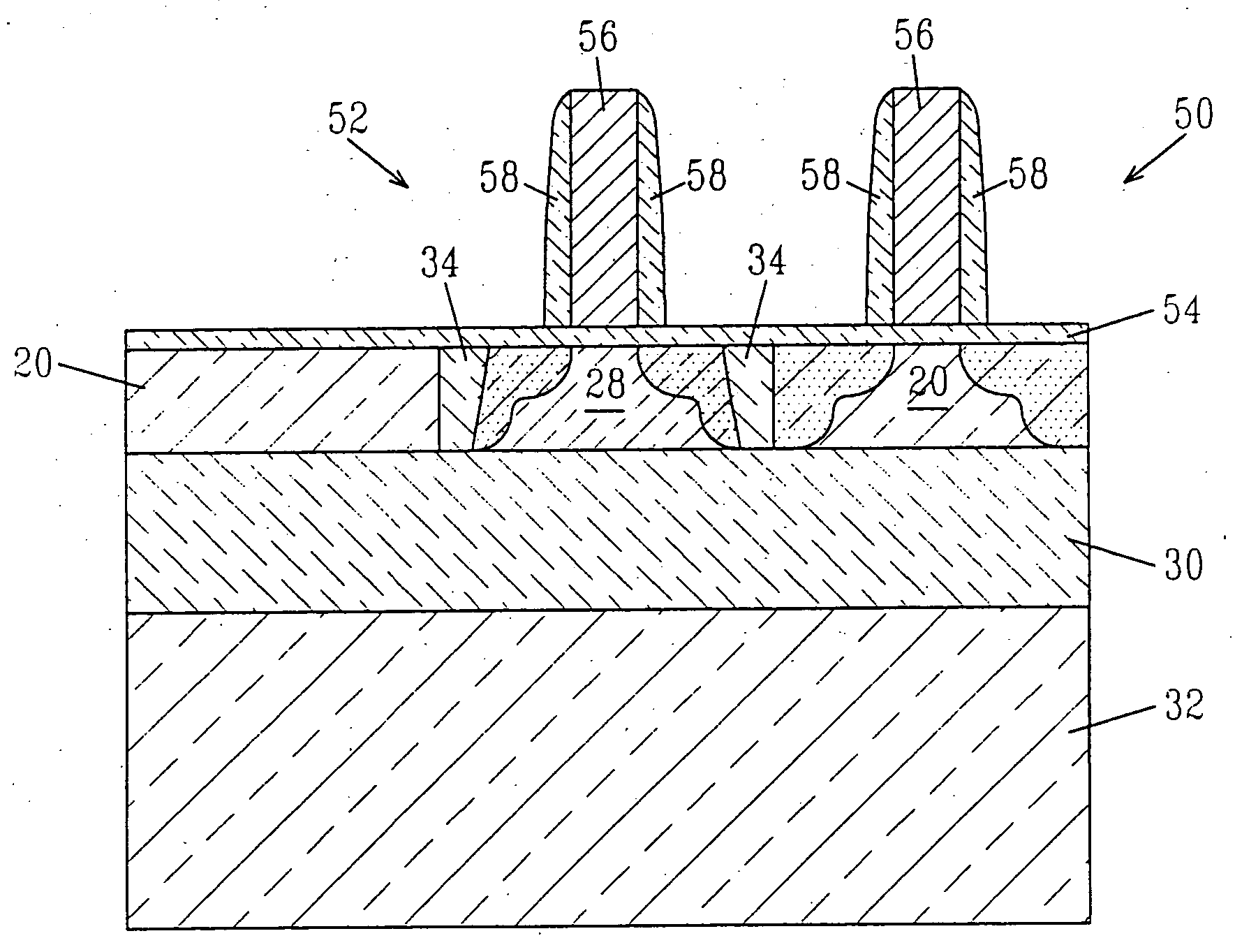
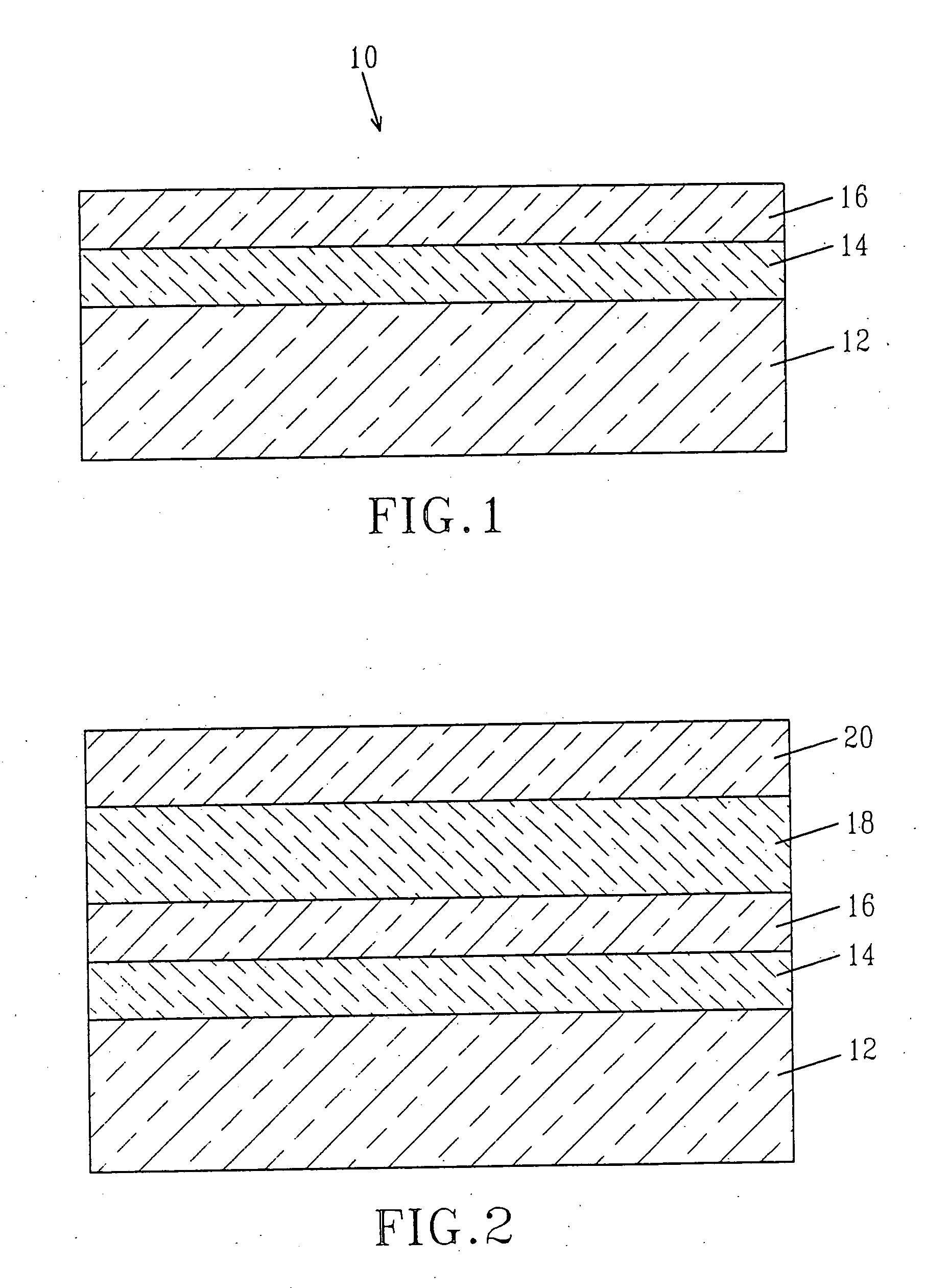
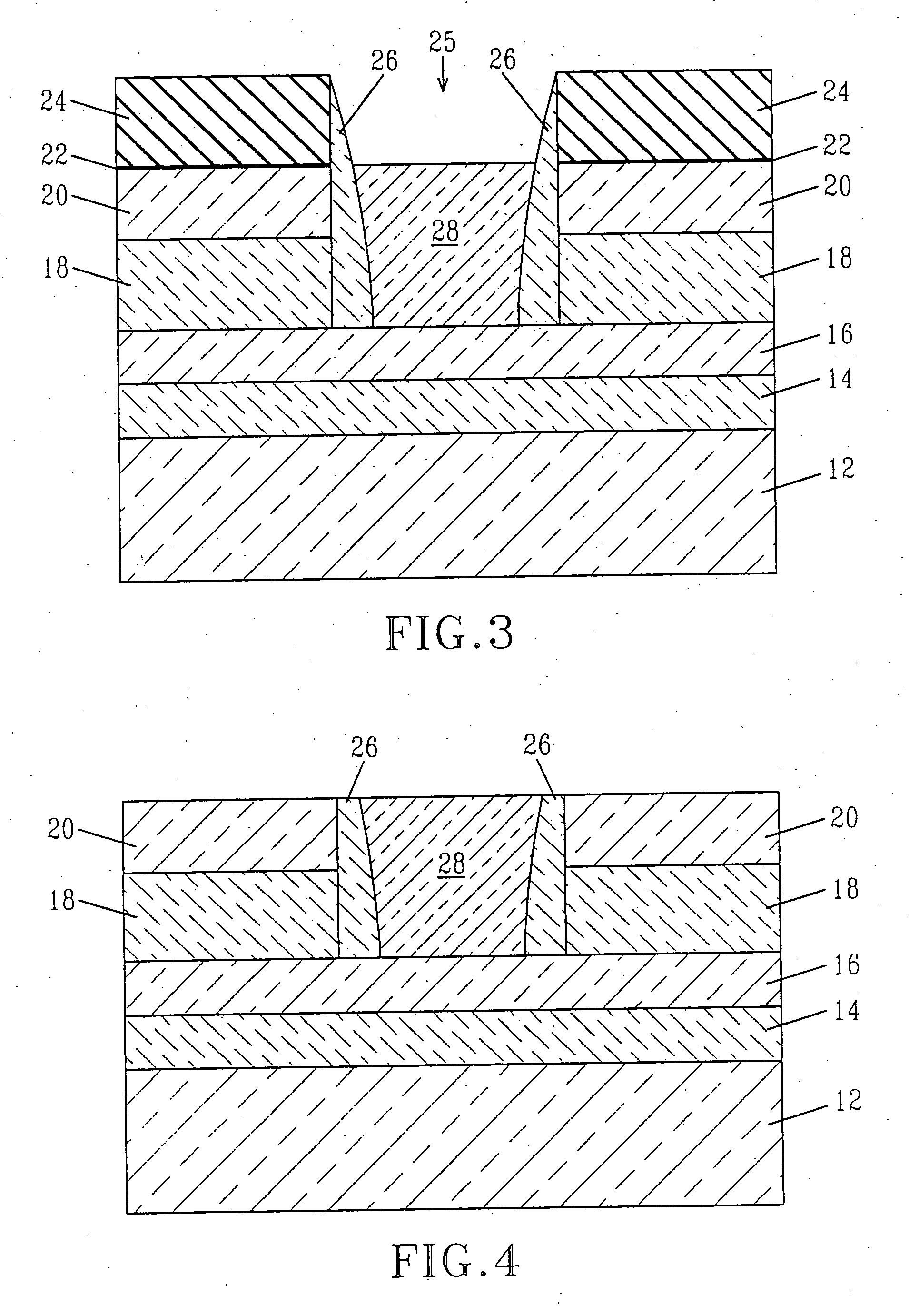
[0032] The present invention, which provides a method of forming an SOI structure with the same thickness of the top SOI layer across the entire wafer where some area contains different crystal orientations and / or materials from the rest of the area, will now be described in greater detail by referring to the drawings that accompany the present application. In the accompanying drawings, like and corresponding elements are referred to by like reference numerals.

[0033] Referring to FIG. 1 there is shown an initial substrate 10 that is employed in the present invention. Initial substrate 10 comprises a carrier wafer 12, an optional etch stop layer 14 located on the carrier wafer 12, and a first semiconductor layer 16 of a first crystal orientation on the optional etch stop layer 14. In embodiments in which the optional etch stop layer 14 is not present, the first semiconductor layer 16 is located directly on the carrier wafer 12.

[0034] Carrier wafer 12 is comprised of any semiconduct...


PUM


Abstract

The invention provides integrated semiconductor devices that are formed upon an SOI substrate having different crystal orientations that provide optimal performance for a specific device. Specifically, an integrated semiconductor structure including at least an SOI substrate having a top semiconductor layer of a first crystallographic orientation and a semiconductor material of a second crystallographic orientation, wherein the semiconductor material is substantially coplanar and of substantially the same thickness as that of the top semiconductor layer and the first crystallographic orientation is different from the second crystallographic orientation is provided. The SOI substrate is formed by forming an opening into a structure that includes at least a first semiconductor layer and a second semiconductor layer that have different crystal orientations. The opening extends to the first semiconductor layer. A semiconductor material is epitaxial grown in the opening and then various etching and etch back processing steps are used in forming the SOI substrate.

Description

[0001] This application is related to co-pending and co-assigned U.S. patent application Ser. No. 10 / 250,241, filed Jun. 23, 2003, the entire content of which is incorporated herein by reference.FIELD OF THE INVENTION [0002] The present invention relates to high-performance metal oxide semiconductor field effect transistors (MOSFETs) for digital or analog applications, and more particularly to MOSFETs utilizing carrier mobility enhancement from substrate surface orientation. BACKGROUND OF THE INVENTION [0003] In present semiconductor technology, complementary metal oxide semiconductor (CMOS) devices, such as nFETs (i.e., n-channel MOSFETs) or pFETs (i.e., p-channel MOSFETs), are typically fabricated upon semiconductor wafers, such as Si, that have a single crystal orientation. In particular, most of today's semiconductor devices are built upon Si having a (100) crystal orientation. [0004] Electrons are known to have a high mobility for a (100) Si surface orientation, but holes are k...

Claims


Application Information

Patent Timeline
IPC IPC(8): H01L21/336H01L21/762H01L21/84H01L27/12H01L29/04H01L29/10H01L29/786
CPCH01L21/76264H01L21/76278H01L21/84H01L27/1203H01L29/78684H01L29/1054H01L29/66772H01L29/78654H01L29/045
Inventor IEONG, MEIKEIYANG, MIN
Owner GLOBALFOUNDRIES US INC
Why Eureka
Try Eureka