

High-frequency chip packages
a technology of high-frequency chips and packaging, which is applied in the direction of program/content distribution protection, instrument details, and semiconductor/solid-state device details, can solve the problems that rf chips typically generate substantial amounts of heat, and achieve the effects of reducing the height of the assembly, simplifying the connection procedure, and improving the electrical performance of the completed assembly
- Summary
- Abstract
- Description
- Claims
- Application Information
AI Technical Summary
Benefits of technology
Problems solved by technology
Method used
Image

Examples
Embodiment Construction
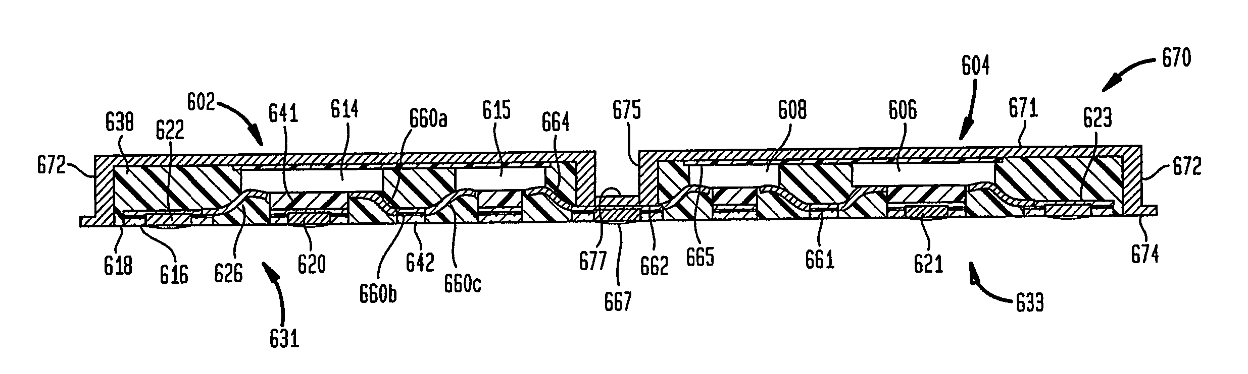
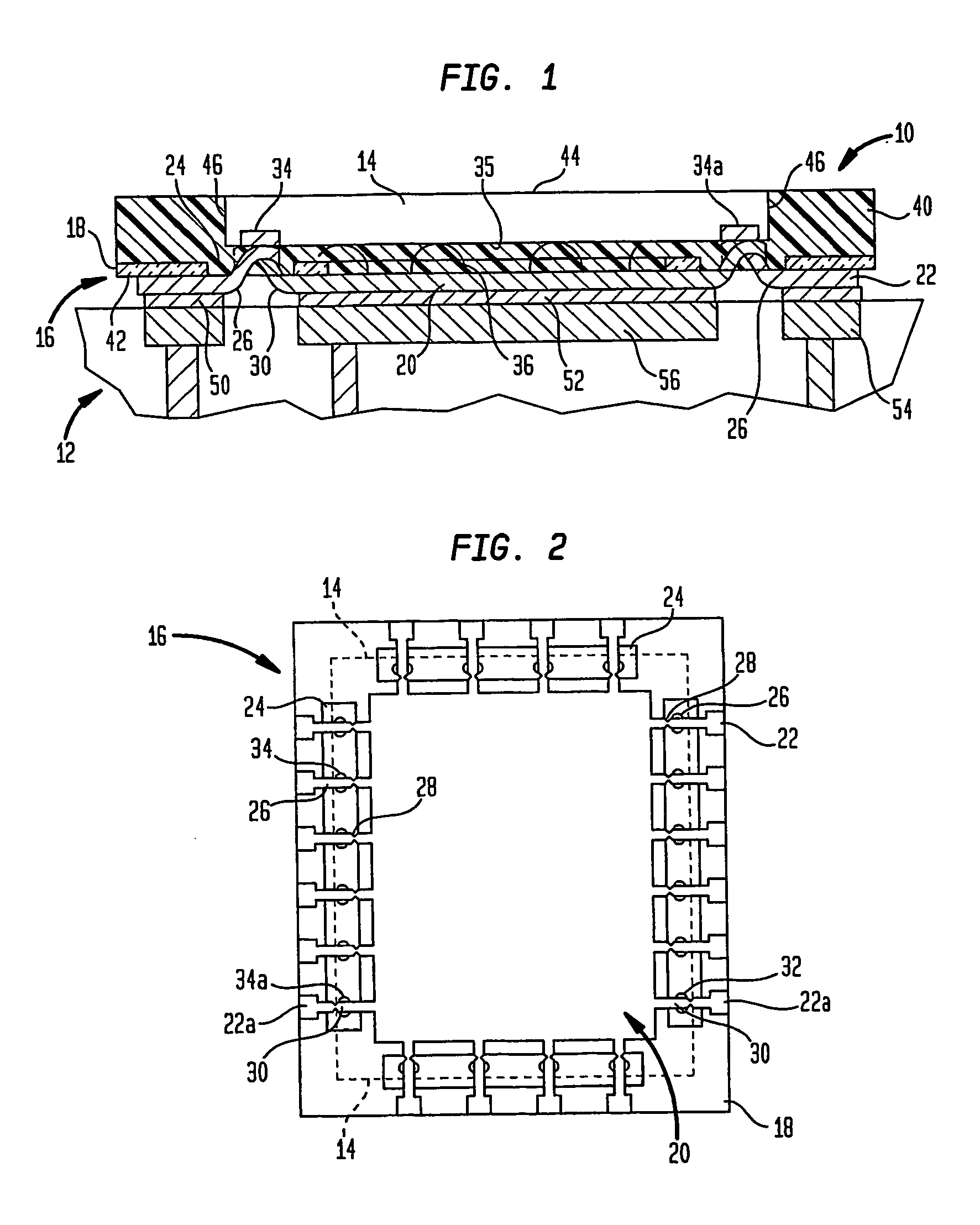
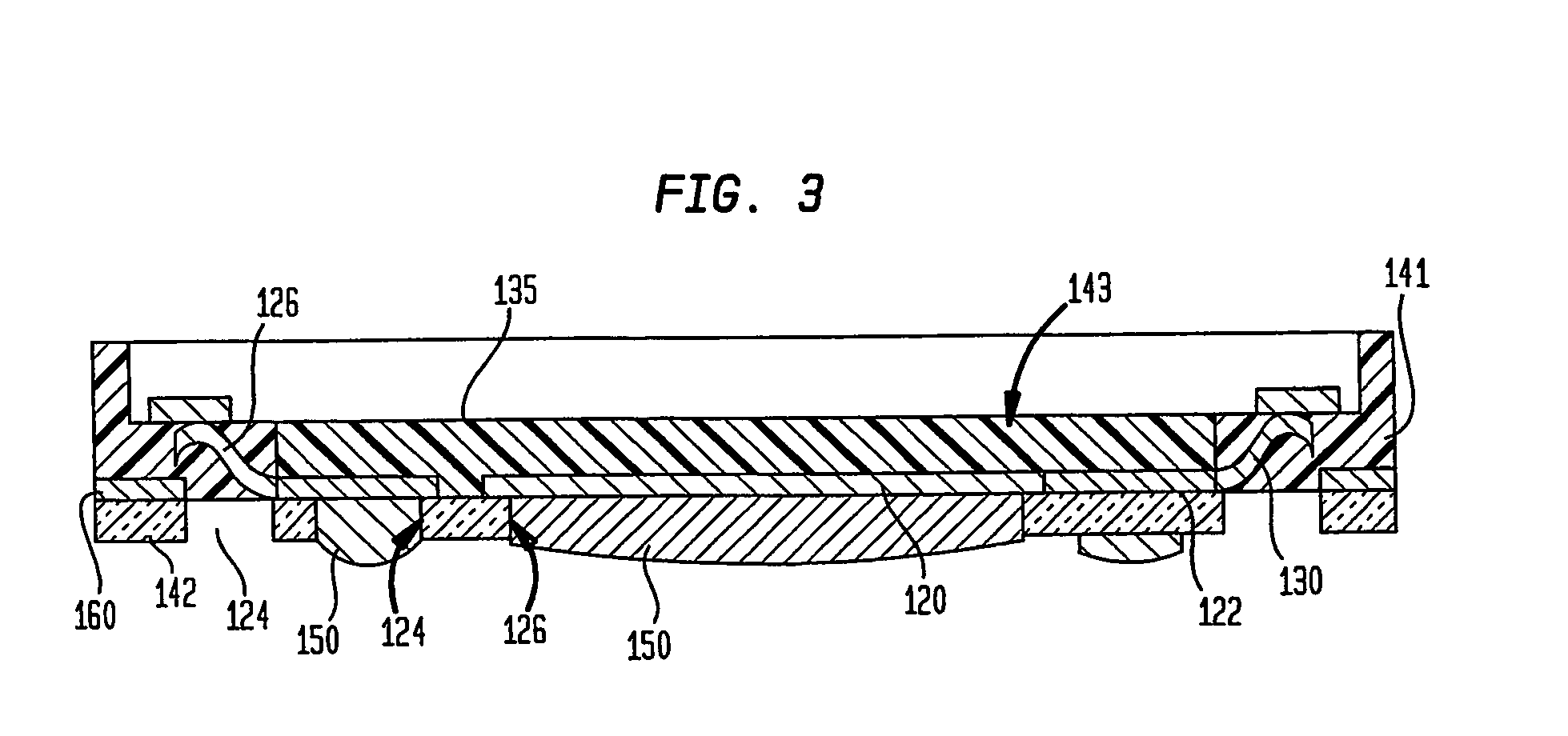
[0048]FIG. 1 shows a diagrammatic sectional view of a chip assembly according to one embodiment of the invention. The assembly includes a packaged chip 10 mounted to a circuit board 12. The packaged chip 10 includes a chip or “die”14 and a chip carrier 16. FIG. 2 shows a diagrammatic plan view of the die 14 and chip carrier 16 of FIG. 1 at an intermediate stage during fabrication of the packaged chip. The chip carrier 16 includes a dielectric layer 18 which desirably is a thin, flexible layer of a polymeric dielectric as, for example, polyimide or BT resin. The chip carrier has a large metallic thermal conductor 20 in a central region and a plurality of terminals 22 in a peripheral region surrounding the central region. The dielectric also has apertures or bond windows 24 extending through the dielectric between the terminals and the thermal conductor. Each terminal 22 has a terminal lead 26 associated with it. Each terminal lead 26 has a connection section projecting inwardly from ...
PUM
 Abstract
Description
Claims
Application Information