

Display device and method for manufacturing the same
a technology of a display device and a manufacturing method, applied in the direction of photosensitive materials, discharge tubes, luminescent screens, etc., can solve the problems of reliability, reach a practical use, and the use of light emitting elements using organic materials is often deteriorated, and achieve the effect of sufficient reliability
- Summary
- Abstract
- Description
- Claims
- Application Information
AI Technical Summary
Benefits of technology
Problems solved by technology
Method used
Image

Examples
embodiment mode 1
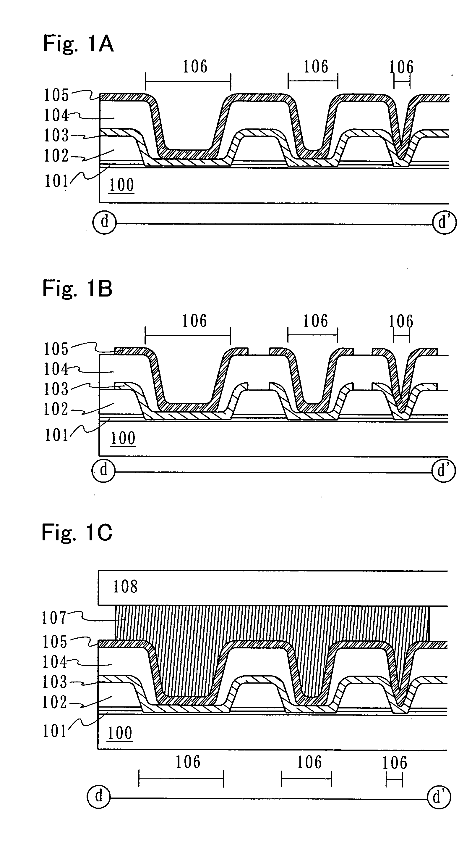
[0070] In an electroluminescent device, an insulating film such as a silicon oxide film, a silicon nitride film, an acrylic film, a polyimide film, or a siloxane film is often used as an interlayer insulating film. Specifically, an acrylic film or a siloxane film is a preferable material since it can be formed by application and it has high planarity. However, it has comparatively high permeability on the other hand.
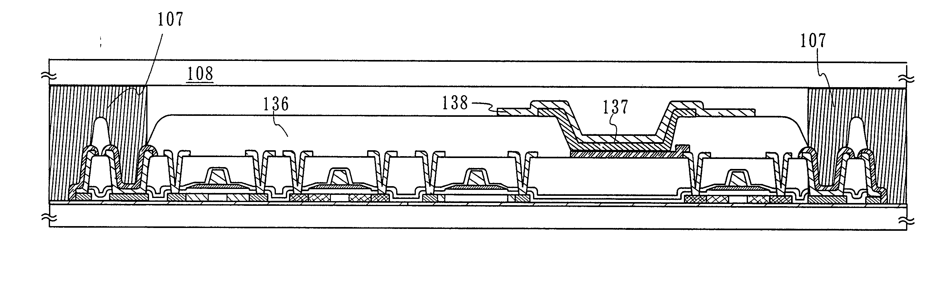
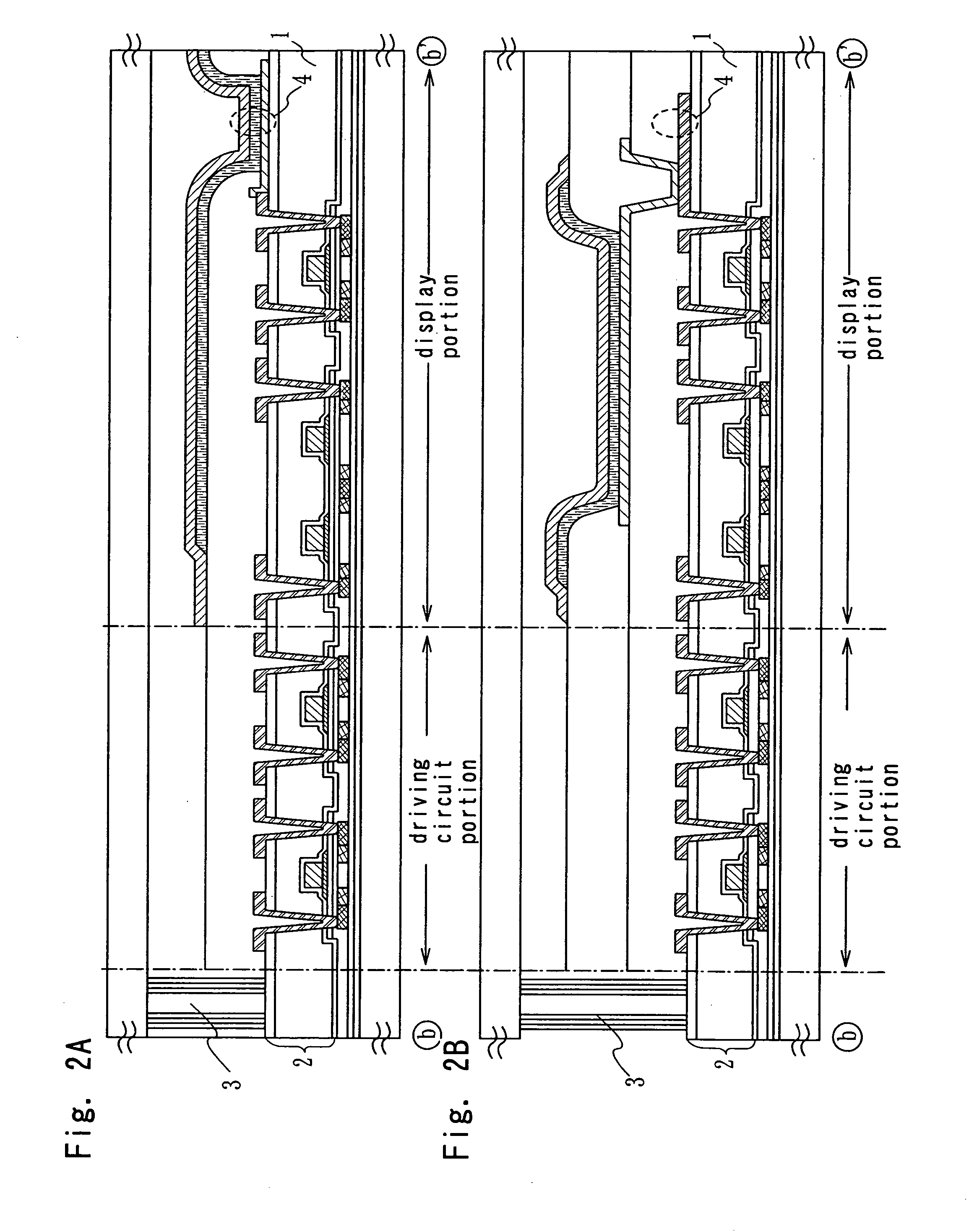
[0071]FIGS. 2A and 2B are cross-sectional views taken along a line b-b′ in FIG. 3. In the case of conventional structures as shown in FIGS. 2A and 2B, an end face 2 of an interlayer insulating film 1 is always exposed to outer atmosphere. Therefore, there is a case that water enters through the interlayer insulating film and deterioration of a light emitting element is caused, even when an upper portion thereof is covered with an impermeable sealant 3 so that a light emitting element 4 is not exposed to outer air.
[0072] Thus, one of structures in the present invention ...
embodiment mode 2
[0082] In this embodiment mode, an example of a structure for preventing water from entering by removing a permeable film on the periphery of a substrate from the periphery of the substrate to a certain distance is described with reference to FIGS. 5A and 5B. Here, the permeable film is assumed an interlayer insulating film. However, an object is not limited to the interlayer insulating film and the present invention can be applied as a countermeasure for the permeable film. The cross-sectional views correspond to a line e-e′ in FIG. 3.
[0083] Reference numeral 120 denotes a portion from which the interlayer insulating films 102 and 104 are removed on an end face of a substrate in FIG. 5A. In Embodiment Mode 1, the end faces of the interlayer insulating films 102 and 104 are exposed to outer air. Then, appropriate distance of the interlayer insulating films 102 and 104 on the end face of the substrate is removed in this embodiment mode, and the end faces thereof are covered with the...
embodiment mode 3
[0088] As is obvious referring to FIGS. 6A to 6C, in the case of manufacturing a sealing structure of the present invention, an opening 106 and an interlayer insulating film removed portion 120 on an end face of a substrate can be formed simultaneously with opening of a contact hole formed in interlayer insulating films 102 and 104, which is effective.
[0089] However, a contact hole is etched under such a condition that the interlayer insulating film and a gate insulating film can be etched using a silicon semiconductor layer as an etching stopper. In the opening 106 and the interlayer insulating film removed portion 120 where an etching stopper does not exist, an etching residue may be generated, or a base insulating film 101 may be sharpened, thereby generating unevenness, in etching the first interlayer insulating film 102.
[0090]FIG. 7A is a SEM picture of a sample in which a siloxane film is formed over a base film as an interlayer insulating film, a silicon nitride film is for...
PUM
 Abstract
Description
Claims
Application Information