Micro-oscillation element
a micro-oscillation element and micro-oscillation technology, applied in the field of micro-oscillation elements, can solve the problems of difficult to achieve high flatness on the entire mirror face over a wide area, high rotational rigidity, and insufficient thinness, so as to prevent the inability to deformation of the oscillation section in the oscillation direction
- Summary
- Abstract
- Description
- Claims
- Application Information
AI Technical Summary
Benefits of technology
Problems solved by technology
Method used
Image
Examples
first embodiment
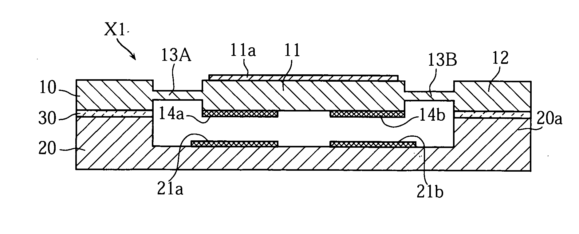
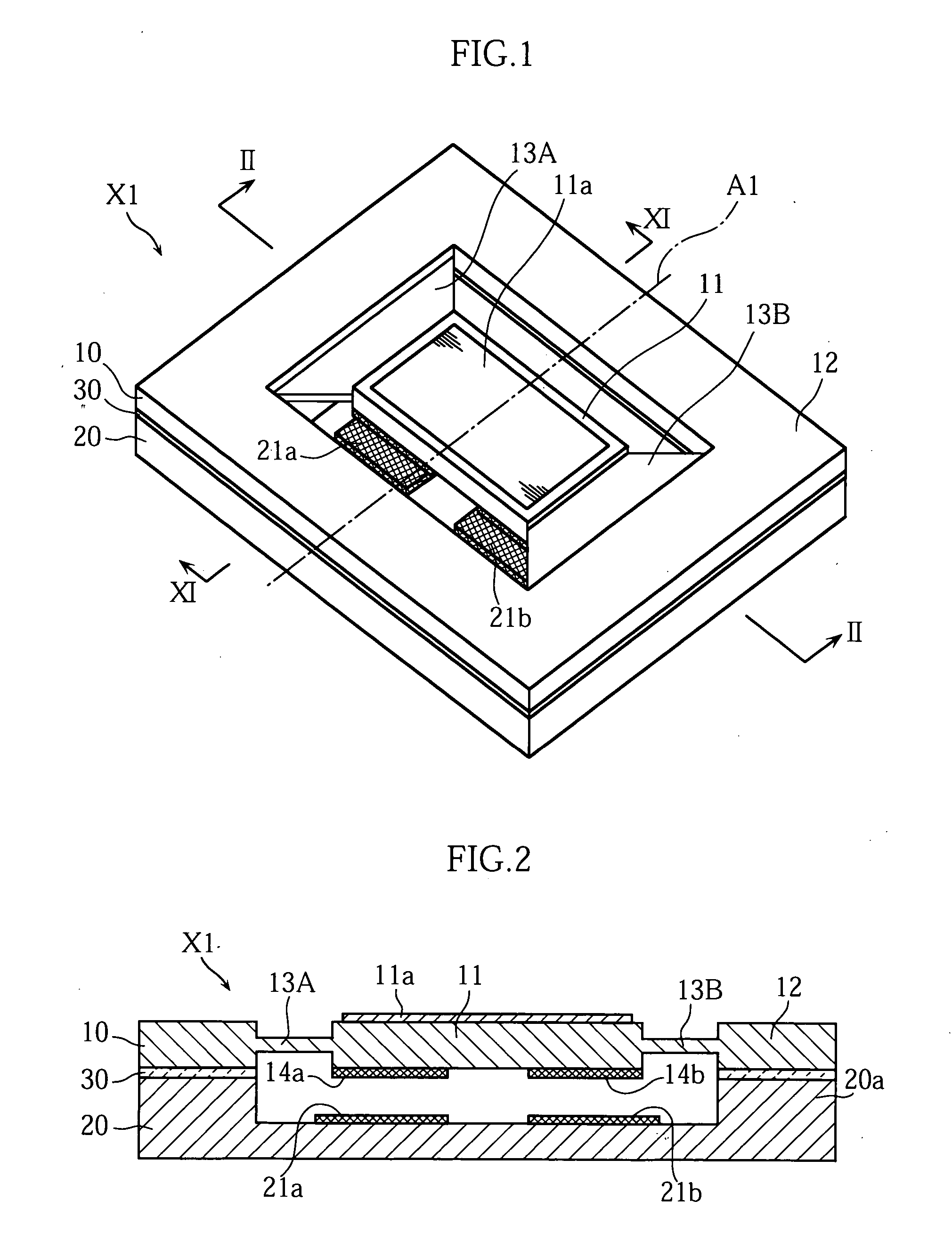
[0062]FIG. 1 and FIG. 2 show the micro-mirror element X1 of the present invention. FIG. 1 is a perspective view of the micro-mirror element X1, and FIG. 2 is a cross-sectional view along the II-II line in FIG. 1. The micro-mirror element X1 has a structure where the mirror substrate 10 and the base substrate 20 are layered via the insulation layer 30.
[0063] The mirror substrate 10 is comprised of a mirror section 11, a frame 12 surrounding this, and a pair of springs 13A and 13B which connect the mirror section 11 and the frame 12. The mirror substrate 10 is formed by bulk micro-machining technology, from a silicon substrate to which conductivity is provided by doping such n-type impurities as P and As, or by such a P-type impurity as B. Specifically, the mirror section 11, the frame 12 and the pair of springs 13A and 13B are formed on a plate type conductive silicon substrate by dry etching or by wet etching, which is performed using a mask for patterning. For the dry etching, Deep...
second embodiment
[0081]FIG. 12 to FIG. 14 show a micro-mirror element X2 according to the present invention. FIG. 12 is a perspective view of the micro-mirror element X2. FIG. 13 is a cross-sectional view along the XIII-XIII line in FIG. 12, and FIG. 14 is a cross-sectional view along the XIV-XIV line in FIG. 12. The micro-mirror element X2 has a structure where the mirror substrate 10 and the base substrate 20 are layered via the insulation layer 30, and the mirror substrate 10 is comprised of a mirror section 11, a frame 12, a pair of springs 13A and 13B, and a pair of torsion bars 15. The difference from the micro-mirror element X1 is that the micro-mirror element X2 has a pair of torsion bars 15, and the rest of the configuration and variant forms thereof are the same as the micro-mirror element X1.
[0082] The pair of torsion bars are connected to the mirror section 11 and the frame 12, and defines the oscillation axis A2 in the oscillation operation of the mirror section 11. Each one of the tors...
third embodiment
[0088]FIG. 17 to FIG. 19 show the micro-mirror element X3 according to the present invention. FIG. 17 is a perspective view of the micro-mirror element X3. FIG. 18 is a cross-sectional view along the XVIII-XVIII line in FIG. 17, and FIG. 19 is a cross-sectional view along the XIX-XIX line in FIG. 17. The micro-mirror element X3 has a structure where the mirror substrate 10 and the base substrate 20 are layered via the insulation layer 30, and the mirror substrate 10 is comprised of a mirror section 11, a frame 12, a pair of springs 13′A and 13′B, and a pair of torsion bars 15′. In the mirror substrate 10, movable electrodes 14′a and 14′b are disposed, and in the base substrate 20, fixed electrodes 21′a and 21′b are disposed. The difference from the micro-mirror element X2 is that the micro-mirror element X3 is comprised of the springs 13′A and 13′B, movable electrodes 14′a and 14′b, fixed electrodes 21′a and 21′b, and a pair of torsion bars 15′, instead of the springs 13A and 13B, m...
PUM
 Abstract
Description
Claims
Application Information


