Method of manufacturing a transistor

a manufacturing method and transistor technology, applied in the direction of semiconductor devices, basic electric elements, electrical appliances, etc., can solve the problems of junction leakage current and gate control loss of transistors, and achieve the effect of preventing junction leakage current and reducing annealing process

Inactive Publication Date: 2005-03-03
SAMSUNG ELECTRONICS CO LTD
View PDF13 Cites 46 Cited by
  • Summary
  • Abstract
  • Description
  • Claims
  • Application Information

AI Technical Summary

Benefits of technology

[0031] Embodiments of the invention provide a method of manufacturing a transistor that prevents a junction leakage current by locally ion-implanting a channel adjusting impurity into a channel region after forming a pad polysilicon layer and that substantially reduces an annealing process after the local ion implantation.

Problems solved by technology

These short channel effects cause gate control to be lost from the transistor.
This annealing hastens a diffusion of the ion-implanted impurity to change a threshold value or increase a PN junction area or junction density and thus causes a junction leakage current.
However, the above conventional transistor manufacturing method exhibits the following problems.

Method used


Image

  • Method of manufacturing a transistor
  • Method of manufacturing a transistor
  • Method of manufacturing a transistor

Examples


Embodiment Construction

[0036] Hereinafter, examplary embodiments of the invention will be described in detail with reference to FIGS. 2 to 3. This invention may be embodied in many different forms and should not be construed as being limited to the example embodiments set forth herein; rather, these example embodiments are provided so that this disclosure is thorough and complete, and conveys the concept of the invention to those skilled in the art.

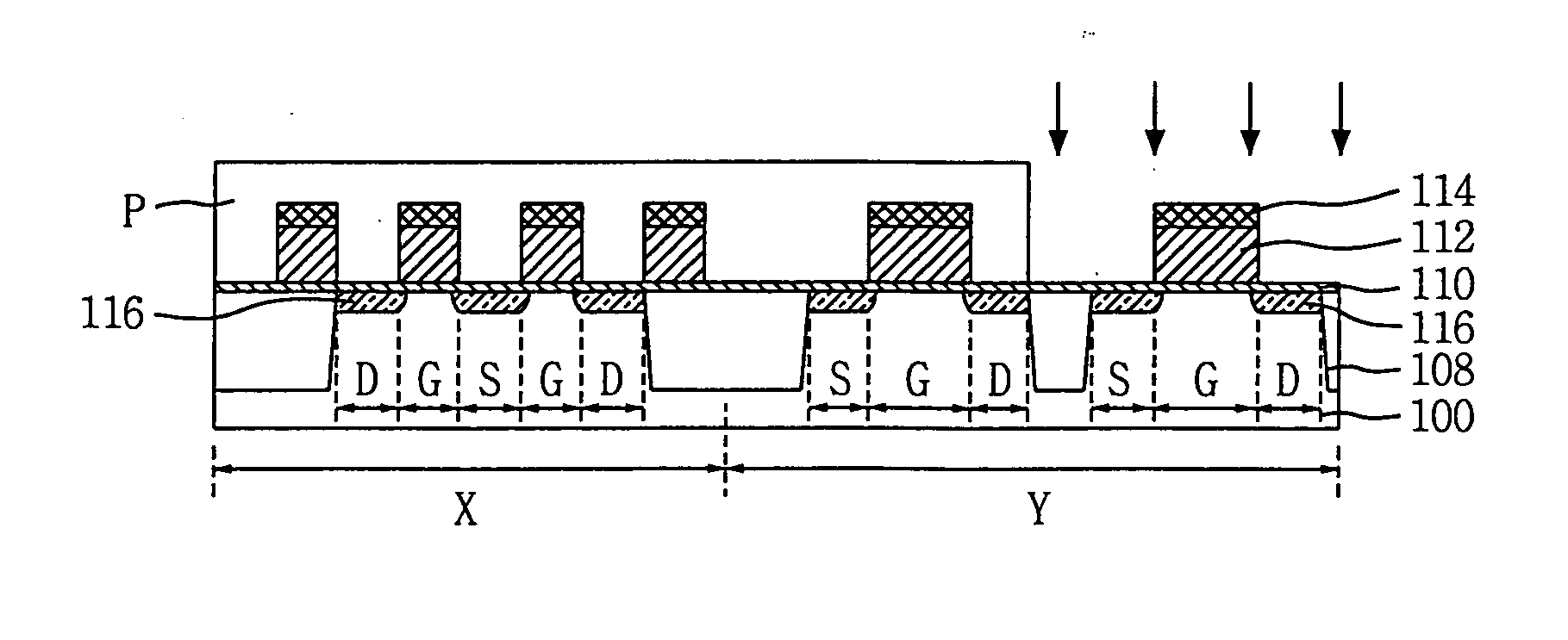
[0037]FIGS. 2a to 2x are cross-sectional diagrams illustrating a transistor manufacturing process according to some embodiments of the invention.

[0038] Referring to FIG. 2a, a pad oxide layer 102, a molding polysilicon layer 104, and a hard mask layer 106 are sequentially formed on a semiconductor substrate 100. The molding polysilicon layer 104 is formed through a chemical vapor deposition (CVD), and the hard mask layer 106 is formed of silicon nitride or silicon oxide nitride on the semiconductor substrate 100 by in-situ in the same chamber when forming the...


PUM


Abstract

A method of manufacturing a transistor according to some embodiments includes sequentially forming a dummy gate oxide layer and a dummy gate electrode on an active region of a semiconductor substrate, ion-implanting a first conductive impurity into source/drain regions to form first impurity regions, and ion-implanting the first conductive impurity to form second impurity regions that are overlapped by the first impurity regions. The method includes forming a pad polysilicon layer on the source/drain regions, sequentially removing the pad polysilicon layer and the dummy gate electrode from a gate region of the semiconductor substrate, annealing the semiconductor substrate, and ion-implanting a second conductive impurity to form a third impurity region in the gate region. The method includes removing the dummy gate oxide layer, forming a gate insulation layer, and forming a gate electrode on the gate region.

Description

CROSS REFERENCE TO RELATED APPLICATIONS [0001] This application claims priority from Korean Patent Application No. 2003-60331, filed on Aug. 29, 2003, the contents of which are herein incorporated by reference in their entirety for all purposes. BACKGROUND OF THE INVENTION [0002] 1. Technical Field of the Invention [0003] This disclosure relates to methods of manufacturing semiconductor devices, and more particularly, to a transistor manufacturing method that substantially reduces an annealing process after a local ion implantation of channel adjusting impurity, that controls a thermal ion diffusion of the channel adjusting impurity, and that prevents a junction leakage current. [0004] 2. Description of the Related Art [0005] The continuous advancement for increased integration levels in semiconductor devices requires a miniaturization in the size of transistor components. Accordingly, as a length of a channel is reduced from a conventional long channel to a short channel under 0.5 ...

Claims


Application Information

Patent Timeline
Patent Type & Authority Applications(United States)
IPC IPC(8): H01L21/336H01L21/8234H01L21/8238H01L21/334
CPCH01L21/823425H01L21/823814H01L29/66545H01L21/82385H01L29/66537H01L21/823828H01L21/18
Inventor YOON, JAE-MANPARK, DONG-GUNYOSHIDA, MAKOTOJIN, GYO-YOUNGCHOE, JEONG-DONGHAN, SANG-YEON
Owner SAMSUNG ELECTRONICS CO LTD
Why Eureka
Try Eureka