Plating apparatus and plating method

a technology of plating apparatus and plating solution, which is applied in the direction of coatings, electrolysis components, electrolysis processes, etc., can solve the problems of difficult difficulty in handling the plating solution, and air bubbles attracted to the hydrophobic surface, etc., to achieve the effect of easy handling and relatively easy control of the composition of the plating solution

Inactive Publication Date: 2005-03-10
EBARA CORP
View PDF14 Cites 40 Cited by
  • Summary
  • Abstract
  • Description
  • Claims
  • Application Information

AI Technical Summary

Benefits of technology

[0013] The present invention has been made in view of the above situation in the related art. It is therefore a first object of the present invention to provide a plating apparatus having a porous memb

Problems solved by technology

Therefore, the plating solution is less liable to infiltrate through the porous member, and it is tedious and time-consuming to handle the plating solution when it is to penetrate into the porous member.
Once entrapped in the porous member, the air bubbles are attracted to the hydrophobic surface and cannot easily be removed from the porous member.
Furthermore, additives and a surfactant added to the plating solution are apt to be attracted to the surface of the hydrophobic material, making it difficult to control the composition of the plating solution.
In the prior art, when plating is performed, the amount of plated material is different in regions of the surface of the substrate depending on the shape of the interconnect pattern under the influence of distribution of current density or the influence of additives, and hence it is difficult to form a plated film having a uniform thickness over the entire surface of the substrate.
As a result, in a case where an interconnect pattern is filled entirely with interconnect material such as copper by plating, the thickness of a plated film differs depending on t

Method used


Image

  • Plating apparatus and plating method
  • Plating apparatus and plating method
  • Plating apparatus and plating method

Examples


Embodiment Construction

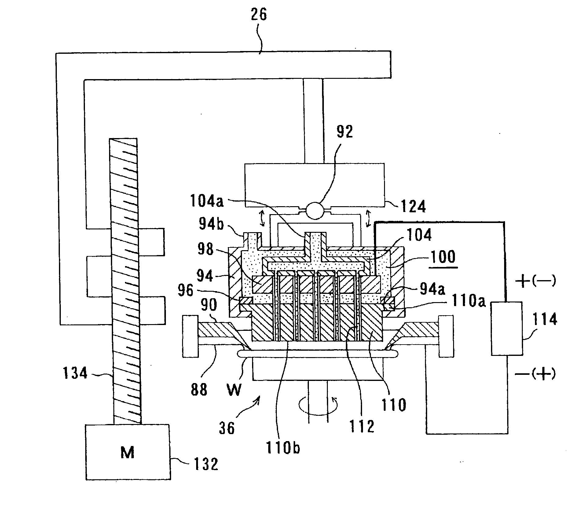
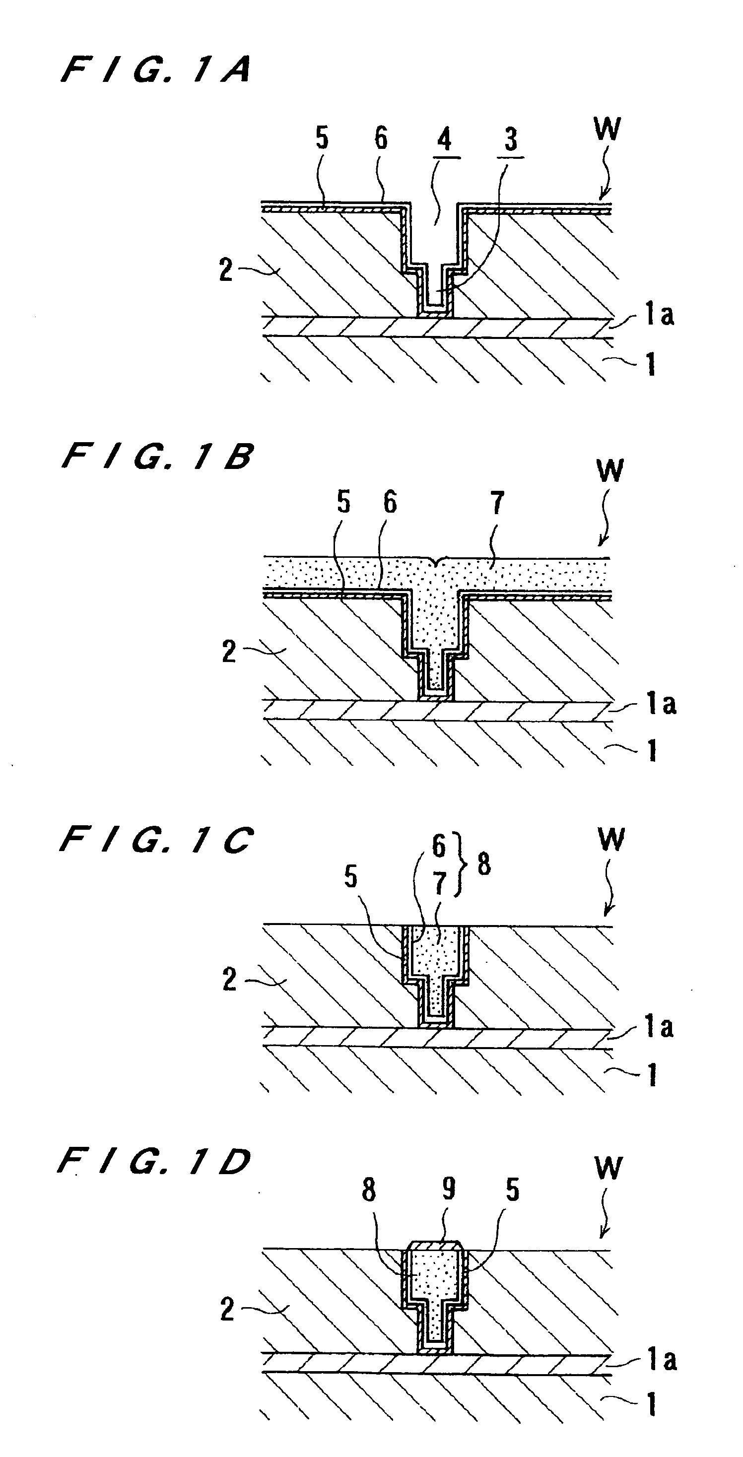
[0154] Preferred embodiments of the present invention will be described below with reference to the drawings. The following embodiments show examples in which copper as an interconnect material is embedded in fine recesses for interconnects formed in a surface of a substrate such as a semiconductor wafer by plating so as to form interconnects composed of a copper layer. However, it should be noted that other kinds of interconnect materials may be used instead of copper.

[0155]FIGS. 1A through 1D illustrate an example of forming copper interconnects in a semiconductor device. As shown in FIG. 1A, an insulating film 2, such as an oxide film of SiO2 or a film of low-k material, is deposited on a conductive layer 1a formed on a semiconductor base 1 having formed semiconductor devices. Via holes 3 and trenches 4 are formed in the insulating film 2 by performing a lithography / etching technique so as to provide fine recesses for interconnects. Thereafter, a barrier layer 5 of TaN or the li...


PUM

PropertyMeasurementUnit
Timeaaaaaaaaaa
Distanceaaaaaaaaaa
Pressureaaaaaaaaaa

Abstract

A plating apparatus is used for filling a fine interconnect pattern formed in the substrate with metal to form interconnects. The plating apparatus includes a substrate holder for holding a substrate, a cathode portion including a sealing member for contacting a peripheral portion of a surface, to be plated, of the substrate held by said substrate holder to seal said peripheral portion water-tightly, and a cathode for contacting the substrate to supply current to the substrate, an anode vertically movably disposed so as to face the surface, to be plated, of the substrate, and a porous member disposed between said anode and the surface, to be plated, of the substrate, said porous member being made of a water-retentive material, wherein said porous member has at least a hydrophilic substrate-facing surface which faces the surface, to be plated, of the substrate.

Description

BACKGROUND OF THE INVENTION [0001] 1. Field of the Invention [0002] The present invention relates to a plating apparatus and a plating method, and more particularly to a plating apparatus and a plating method used for filling a fine interconnect pattern formed in a substrate, such as a semiconductor substrate, with metal (interconnect material) such as copper so as to form interconnects. [0003] 2. Description of the Related Art [0004] Recently, as a circuit forming method, the so-called “damascene process”, which comprises forming fine recesses for interconnects, such as trenches or via holes in a circuit form, in a semiconductor substrate, embedding the fine recesses with copper (interconnect material) by copper plating, and removing a copper layer (plated film) at portions other than the fine recesses by CMP means or the like, has been employed. In this damascene process, from the viewpoint of reducing loads on subsequent CMP, it is desirable that a copper plated film be deposited...

Claims


Application Information

Patent Timeline
IPC IPC(8): B05D5/12C25D5/00C25D7/12C25D17/00H01L21/288H01L21/768
CPCH01L21/2885H01L21/76877C25D5/003C25D17/001C25D17/002C25D7/123
Inventor KURASHINA, KEIICHINAGAI, MIZUKIYAMAMOTO, SATORUKANDA, HIROYUKIMISHIMA, KOJINAKADA, TSUTOMU
Owner EBARA CORP
Why Eureka
Try Eureka