Light emitting electronic component

Inactive Publication Date: 2005-03-10
POLYMATECH CO LTD
View PDF10 Cites 17 Cited by
  • Summary
  • Abstract
  • Description
  • Claims
  • Application Information

AI Technical Summary

Benefits of technology

[0010] An object of the invention is to provide a key pad which uses a desirable EL panel with respect to uniformity and intensity

Problems solved by technology

Since contacts used for switching operations are provided beneath each key top, the back lighting cannot be provided.
Accordingly, LEDs are disposed in between adjacent key tops, however the light emitted from the LEDs cannot sufficiently transmit to the key tops with the result of insufficient overall illumination efficiency due to lack of uniformity in brightness of adjacent keys.
While electroluminescent devices include organic electroluminescent device and inorganic electroluminescent device, inorganic electroluminescent devices are often used in applications for push button switches because they do not react very sensitively to moisture in the atmosphere.
The problem of the lack of uniformity in the emitted light and the darkness in the case of using LEDs for the backlighting of the key tops are not found in the above conventional art since the electroluminescent light emitting portion emits light beneath each key top.
However, since the above switches have structures, which deform by pushing the electroluminescent panels in operations, the electroluminescent light emitting portions are subjected to bending load.
Further, when structures in which a portion of the electroluminescent device is pushed by a hard key top are used, any

Method used


Image

  • Light emitting electronic component
  • Light emitting electronic component
  • Light emitting electronic component

Examples


example 1

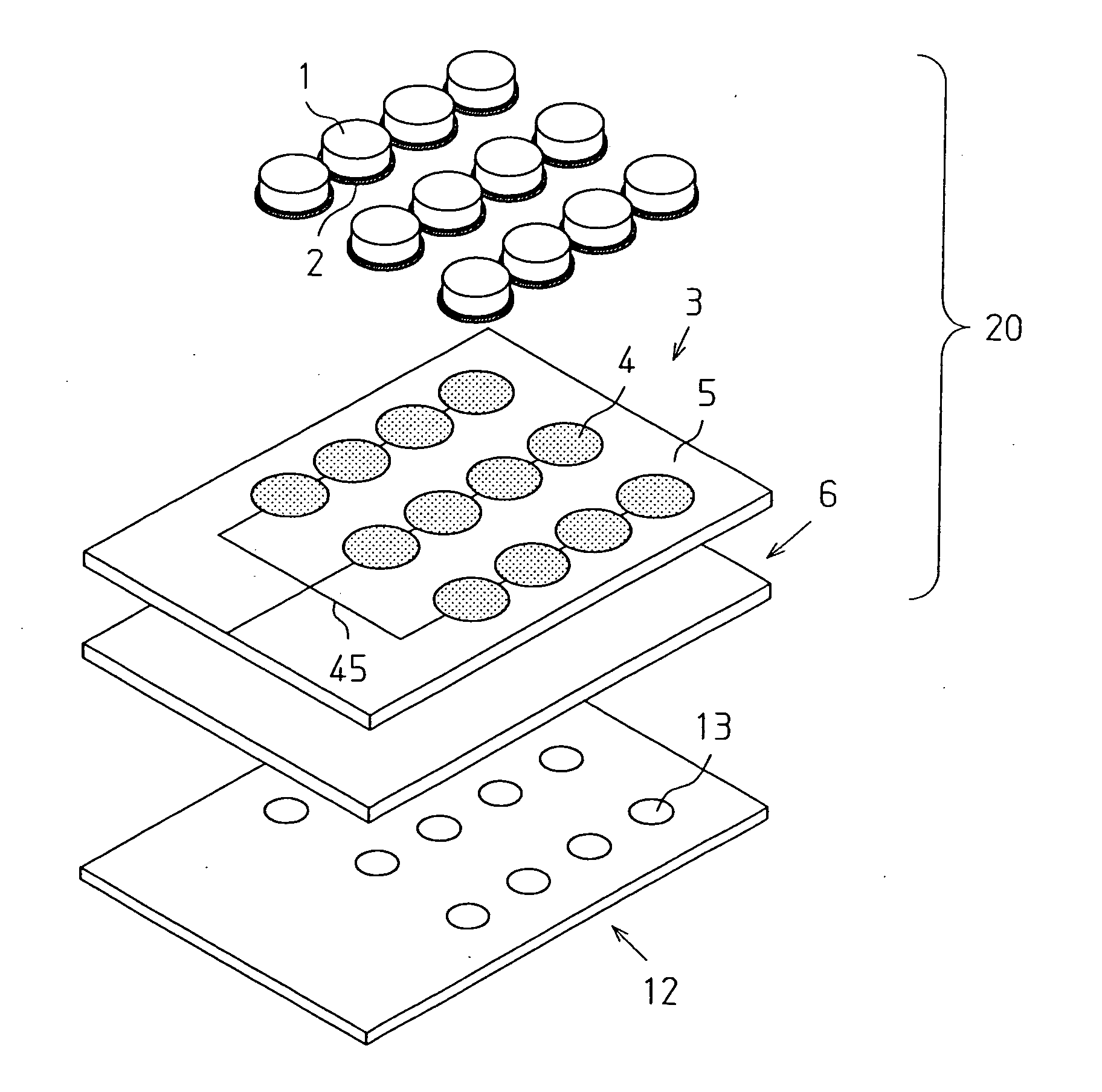
[0055] The translucent molding 1 shown in FIG. 4 is fabricated by injection molding of polycarbonate resin which transmits visible rays. The indicator layer 2 is formed on the bottom surface of the translucent molding 1 by printing light transmitting ink.

[0056] An ITO film (manufactured by Oji Tobi Co., OTEC-120), which comprises the film substrate 11, and an ITO thin film provided thereon to be used as the transparent electrode 41 was prepared. The emitting layer 42 was printed from a blue green colored fluorescent paste (manufactured by DuPont, 7151) and the dielectric layer 43 was printed from a dielectric paste (manufactured by DuPont). The backside electrode layer 44 was formed by thermocompression of an aluminum foil having 0.025 mm thickness. Then the insulative resist layer 46 was provided to cover the electrode. The EL panel 3 was thereby fabricated with the light emitting portion 4.

[0057] The vibration absorbing sheet comprising silicone rubber and having a semi-spherica...

example 2

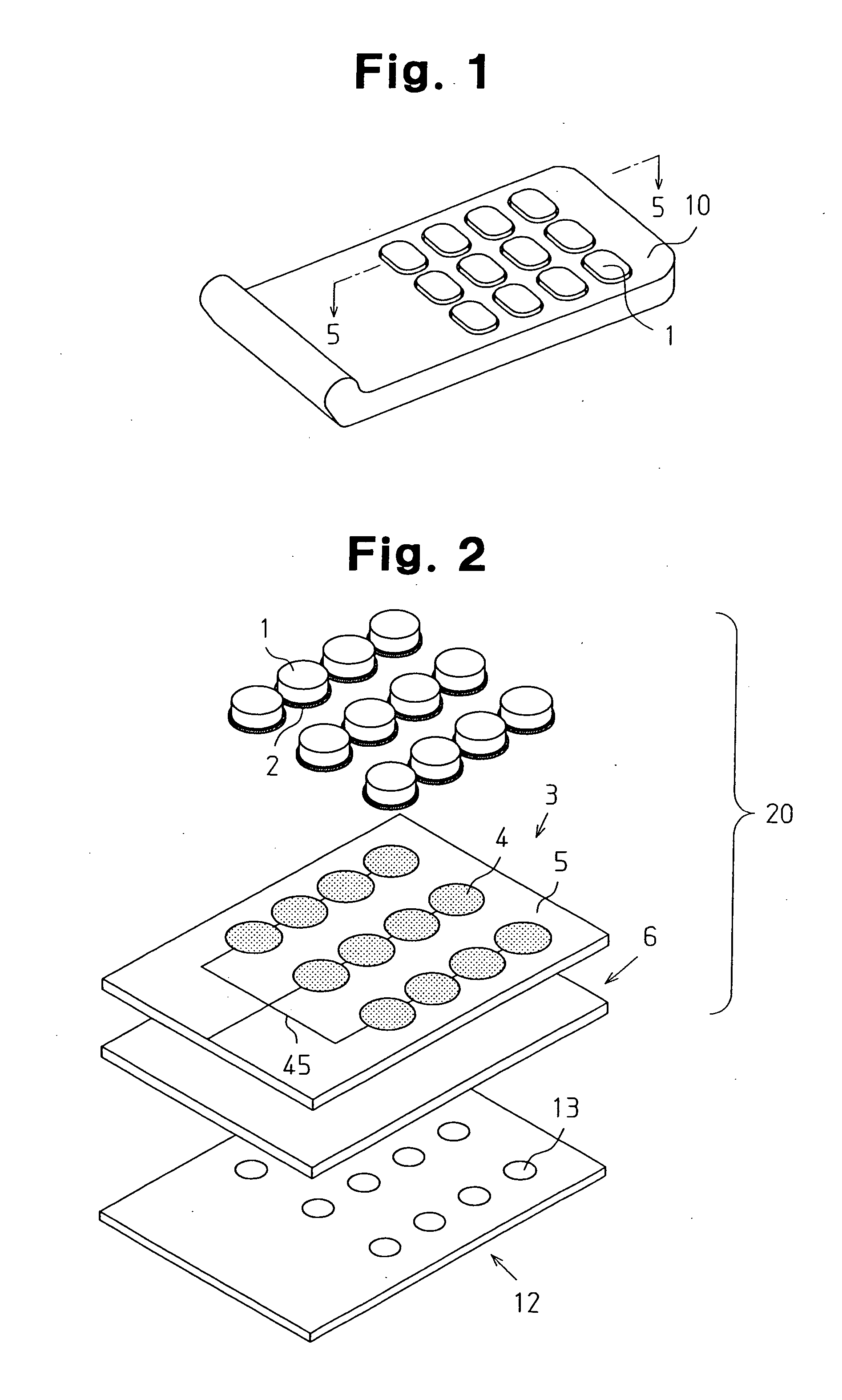
[0062] The translucent molding 1 shown in FIG. 3 was fabricated by injection molding of visible light transparent polycarbonate resin in a similar manner as Example 1. The indicator layer 2 was formed by printing light transmitting paint on the bottom surface of the translucent molding 1.

[0063] The method for producing the EL panel 3 having the EL light emitting portions 4 shown in FIG. 8(a) is described as follows. The EL panel 3 was fabricated by using a fluoride resin plate for providing sufficient strength during process steps. The fluoride resin plate is removed from the EL panel 3 after completing fabrication. In order to form the light emitting portion 4 in the same shape as the contour of the bottom surface of the translucent molding 1 over the fluoride resin plate, the transparent electrode layer 41 was formed from an ITO paste for transparent electrodes (manufactured by DuPont), the emitting layer 42 was formed from blue-green colored fluorescent paste (manufactured by Du...

example 3

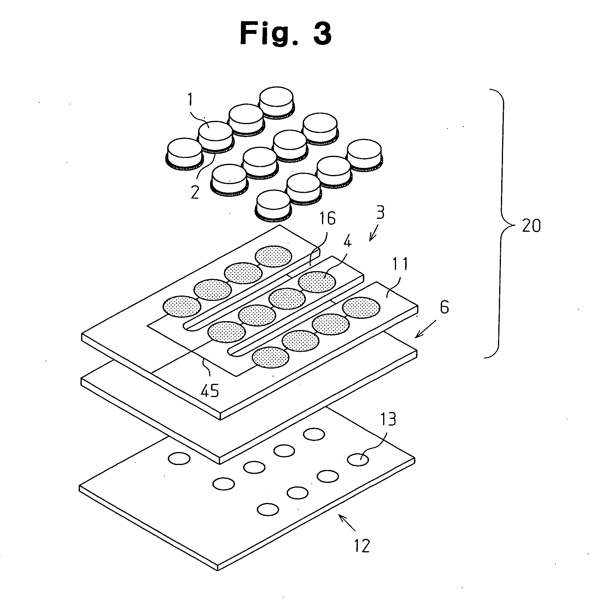
[0068]FIG. 8(c) is referred to. The key pad of Example 3 was formed similarly to that of Example 2 except that the structure of the EL panel 3 differs in Example 3. The EL panel 3 of Example 3 uses a resin film 11 comprising polyethylene terephthalate having flexibility and an insulative property for the substrate and the substrate was not removed after finishing the EL panel 3.

[0069] The method for producing the EL panel 3 is described below. The transparent electrode layer 41 of the EL light emitting portion 4 was formed by etching the ITO film (manufactured by Oji Tobi Co. under the trade name of OTEC-120) formed on one surface of the substrate. The emitting layer 42 was formed by blue green color fluorescent paste (manufactured by Fujikura Kasei), the dielectric layer 43 was formed by a dielectric paste (manufactured by Fujikura Kasei) and the backside electrode layer 44 was formed by paste for carbon electrodes (manufactured by Fujikura Kasei) in this order to form a plurality...


PUM


Abstract

A light emitting electronic component, in which light emitted by an electroluminescent panel is visible through a translucent molding. The electroluminescent panel comprises an electroluminescent light emitting region having a first surface and a second surface opposite to the first surface and a non-emitting region. The electroluminescent light emitting region comprises a transparent electrode layer, an emitting layer, a dielectric layer and a backside electrode layer. The translucent molding is disposed in contact with the first surface of the electroluminescent light emitting region. The light emitting electronic component comprises a vibration absorbing sheet disposed in contact with the second surface of the electroluminescent light emitting region so as to absorb vibration which is generated during light emission of the electroluminescent panel.

Description

BACKGROUND OF THE INVENTION [0001] The present invention relates to a light emitting component used for an electronic appliance such as a mobile phone, a portable information terminal, a remote control used for a household electric appliance and a key board. More specifically, the present invention relates to a key pad that illuminates switches by using electroluminescence materials. [0002] Translucent key pads are widely used for operation of electronic appliances such as mobile phones. A key pad has a translucent resin key top which functions as a switch. In order to identify each key top, indicators such as alphanumeric characters and symbols are provided on the top surface or the bottom surface of the key top. Each switch can be made visible and identifiable by illuminating the indicator provided on the key top by means of back lighting when used under low-light conditions. [0003] Conventionally light emitting diodes (LEDs) are used for the back lighting of translucent key pads....

Claims


Application Information

Patent Timeline
IPC IPC(8): G06F3/02G09F13/22H01H13/70H01B3/02H01H13/14H01H13/83H01J1/62H01J63/04H04M1/22H05B33/14
CPCH01H13/83H01H2009/186H01H2205/026H01H2219/018H04M1/22H01H2221/062H01H2229/028H01H2229/03H01H2219/04H01H13/70
Inventor NAKANISHI, YUTAKA
Owner POLYMATECH CO LTD
Why Eureka
Try Eureka