Method of writing data on a storage device using a probe technique

a data and storage device technology, applied in the field of writing data, can solve the problems of spm, the inability of the solid-state memory device to function as a high-density data writing device, and the inability to obtain a hard disk with a higher writing density, so as to achieve low coercive field, high coercive field, and low voltage

Inactive Publication Date: 2005-03-10
SAMSUNG ELECTRONICS CO LTD
View PDF3 Cites 30 Cited by
  • Summary
  • Abstract
  • Description
  • Claims
  • Application Information

AI Technical Summary

Benefits of technology

[0030] In the present invention, to write data, heat and an electric field are simultaneously applied to a domain of a ferroelectric layer, on which data will be written. The heat applied to the ferroelectric layer can lower the coercive field of the ferroelectric layer so as to switch a domain with a lower voltage. Also, writing data can be performed at high speed by applying the heat and the electric field at the same time. Further, a writing medium having a high coercive field can be used to enhance thermal stability. Thus, a domain of a ferroelectric layer with a high coercive field can be effectively switched, without an electrical breakdown between the probe and layer surface.

Problems solved by technology

Since it is anticipated that the needs for primary storage in hand-held devices will reach a capacity of up to several tens of gigabytes in upcoming years, it is difficult for the solid-state memory device to function as a high-density data writing device, probably due to limitations in the lithography technology.
However, it is currently impossible to obtain a hard disk that has a higher magnetic writing density than that of the 10-GB hard disk, due to the superparamagnetic effect.
However, the memory device using SPM has the following problems.
Therefore, when the voltage applied to both ends of the probe is too high, since an interval between the probe and the ferroelectric layer is extremely small, an electrical breakdown, such as a corona discharge, may occur therebetween.
Thus, it takes much time to write data.
However, a coil for generating the magnetic field and a laser diode for generating heat cannot be located in the same space.
Further, since an interval between a magnetic writing head and a writing medium is very narrow, applying the magnetic field and the heat at the same time is almost impossible.

Method used


Image

  • Method of writing data on a storage device using a probe technique
  • Method of writing data on a storage device using a probe technique
  • Method of writing data on a storage device using a probe technique

Examples


Embodiment Construction

[0037] The present invention will now be described more fully with reference to the accompanying drawings, in which an exemplary embodiment of the invention is shown. In the drawings, the thicknesses of layers or regions may be exaggerated for clarity.

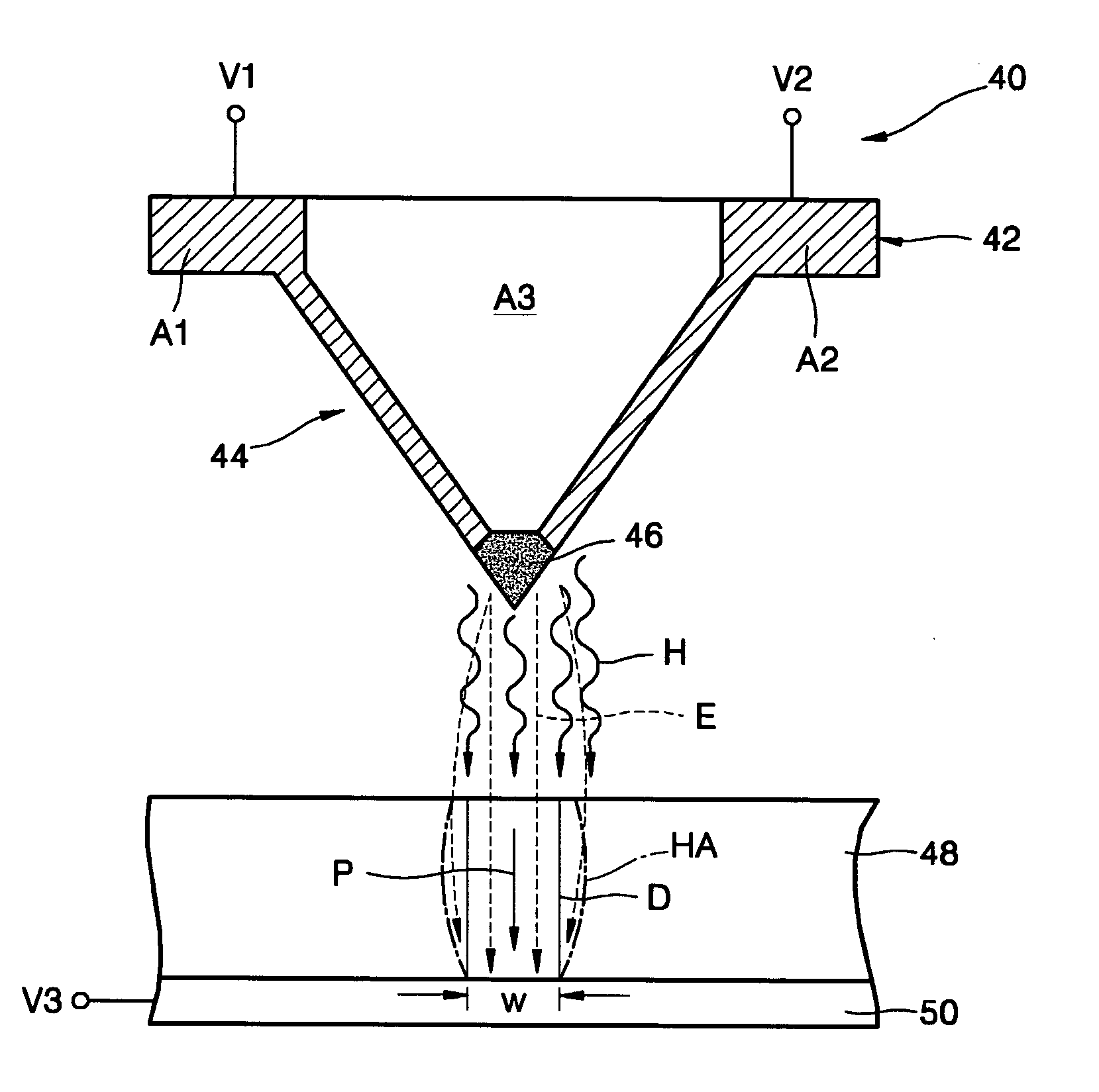
[0038] Referring to FIG. 1, reference numeral 48 denotes a ferroelectric layer used as a data writing medium. Although the ferroelectric layer 48 is preferably a PZT layer, it is possible to use other ferroelectric layers, for example, a BaTiO3 (BTO) layer, a triglycine sulfate (TGS) layer, or a triglycine selenate (TGSe) layer. A lower electrode 50 is disposed on a bottom surface of the ferroelectric layer 48. To write data, a third voltage V3 is applied to the lower electrode 50. A probe 40 is disposed above the ferroelectric layer 48. The probe 40 is positioned at the end of a cantilever (not shown) connected to a power supplier (not shown). The probe 40 comprises a flat panel portion 42, which is connected to the cantilever, and a...


PUM

PropertyMeasurementUnit
resistanceaaaaaaaaaa
temperatureaaaaaaaaaa

Abstract

A method of writing data on a storage device using a probe technique. In the method of writing data on a memory device including a resistive probe used for reading and writing of data, a ferroelectric writing medium on which data is written by the resistive probe, and a lower electrode disposed on a bottom surface of the ferroelectric writing medium, heat and an electric field are applied simultaneously to a domain of the ferroelectric writing medium, on which the data will be written, by applying a voltage to the resistive probe and the lower electrode.

Description

CROSS-REFERENCE TO RELATED APPLICATIONS [0001] This application claims priority from Korean Patent Application No. 2003-62376, filed on Sep. 6, 2003, in the Korean Intellectual Property Office, the disclosure of which is incorporated herein by reference in its entirety. BACKGROUND OF THE INVENTION [0002] 1. Field of the Invention [0003] The present invention relates to a method of writing data, and more particularly, to a method of writing data on a ferroelectric layer using a resistive probe. [0004] 2. Description of the Related Art [0005] Regarding developments in Internet-related technologies, a writing medium on which a large amount of data including motion pictures can be written (hereinafter, referred to as a “high-density writing medium”) and a portable device for writing the data on the writing medium and reading the written data have lately attracted considerable attention as important products on the writing media market. [0006] A portable nonvolatile data writing device c...

Claims


Application Information

Patent Timeline
Patent Type & Authority Applications(United States)
IPC IPC(8): G11B9/14G11B9/00G11B9/02G11B13/00
CPCB82Y10/00G11B9/02G11B9/14G11B2005/0021G11B9/149G11B13/00G11B9/1409
Inventor HONG, SEUNG-BUMKIM, SUNG-DONGJUNG, JU-HWANMIN, DONG-KIPARK, HONG-SIKBAECK, KYOUNG-LOCKPARK, CHUL-MINKIM, YUN-SEOK
Owner SAMSUNG ELECTRONICS CO LTD
Why Eureka
Try Eureka