Method for adaptive segment refinement in optical proximity correction

a technology of optical proximity correction and adaptive segment refinement, which is applied in the field of lithographic processes, can solve the problems of loss of mask shape fidelity, the limit of the lithographic process capacity, and the difficulty in the process of designing tools for automating chip design, and achieve the effect of increasing computation costs

Inactive Publication Date: 2005-03-10
IBM CORP
View PDF18 Cites 60 Cited by
  • Summary
  • Abstract
  • Description
  • Claims
  • Application Information

AI Technical Summary

Benefits of technology

It is therefore an objective of the present invention to provide a method and a computer program product to perform the method, for manufacturing an integrated circuit, including designing a lithographic mask

Problems solved by technology

The advent of advanced lithographic techniques and the attempt of chip manufacturers to closely follow Moore's law predicting an exponential growth of number of components on a chip and their shrinkage on the wafer is making the process of designing tools for automating the chip design extremely challenging.
As the components on the chip become smaller, they are now in the verge of reaching the limits of capacity of the lithographic process.
One of the most common problem of printing integrated circuits on silicon wafers from the mask using lithographic processing is the loss of fidelity of the mask shapes.
The non-linearities associated with this lithographic process of imprinting and the laws of physics associated with light (including diffraction of light waves) makes impressing highly unpredictable.
Since at the early stages in the history of chip manufacturing, the size of the features was still large compared to the wavelength of the light used in the lithographic process, optical proximity effects did not contribute significantly to the total error budget of chip manufacturing.
However, as the size of the features have continued to shrink, mask designers have continuously readapted earlier techniques to obtain the desired results.
Therefore, though prevalent in the early part of the history

Method used


Image

  • Method for adaptive segment refinement in optical proximity correction
  • Method for adaptive segment refinement in optical proximity correction
  • Method for adaptive segment refinement in optical proximity correction

Examples


Embodiment Construction

In the following description, numerous specific details may be set forth to provide a thorough understanding of the present invention. However, it will be obvious to those skilled in the art that the present invention may be practiced without such specific details.

Refer now to the drawings wherein depicted elements are not necessarily shown to scale and wherein like or similar elements are designated by the same reference numeral through the several views.

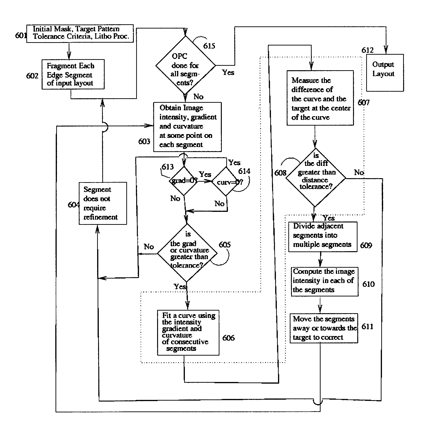
In accordance with the present invention, a method and computer system is provided for performing model-based optical proximity correction (MBOPC), wherein the comparison of simulated image to target image is performed using an adaptive refinement of segmentation that is based on the image gradient. Using this methodology, a proper balance of the segmentation can be achieved that takes into account the variations of the wafer image. This methodology can be used to obtain more accurate and faster image simulation and mask corre...


PUM


Abstract

A method of designing lithographic masks is provided where mask segments used in a model-based optical proximity correction (MBOPC) scheme are adaptively refined based on local image information, such as image intensity, gradient and curvature. The values of intensity, gradient and curvature are evaluated locally at predetermined evaluation points associated with each segment. An estimate of the image intensity between the local evaluation points is preferably obtained by curve fitting based only on values at the evaluation points. The decision to refine a segment is based on the deviation of the simulated image threshold contour from the target image threshold contour. The output mask layout will provide an image having improved fit to the target image, without a significant increase in computation cost.

Description

BACKGROUND OF INVENTION The present invention relates in general to lithographic processes and, more particularly, to a method for correcting a mask layout of an integrated circuit for lithographic processing effects. The advent of advanced lithographic techniques and the attempt of chip manufacturers to closely follow Moore's law predicting an exponential growth of number of components on a chip and their shrinkage on the wafer is making the process of designing tools for automating the chip design extremely challenging. The chip is imprinted by means of optical lithographic techniques on the silicon wafer by way of chrome on glassmasks. As the components on the chip become smaller, they are now in the verge of reaching the limits of capacity of the lithographic process. One of the most common problem of printing integrated circuits on silicon wafers from the mask using lithographic processing is the loss of fidelity of the mask shapes. The dimensions of the wafer shapes are usu...

Claims


Application Information

Patent Timeline
IPC IPC(8): G03F1/14G06F17/50
CPCG03F1/144G06F17/5081G03F1/36G06F30/398
Inventor MUKHERJEE, MAHARAJBAUM, ZACHARYLAVIN, MARK A.SAMUELS, DONALD J.SINGH, RAMA N.
Owner IBM CORP
Why Eureka
Try Eureka