Resonant clock distribution for very large scale integrated circuits

a technology of integrated circuits and clocks, applied in the direction of generating/distributing signals, pulse automatic control, oscillator generators, etc., can solve the problems of increasing the difficulty of clocking large digital chips with a single high-frequency global clock, increasing dynamic power dissipation, and increasing power consumption. , to achieve the effect of efficient distribution of high-speed clock signals

Inactive Publication Date: 2005-03-17
THE TRUSTEES OF COLUMBIA UNIV IN THE CITY OF NEW YORK
View PDF1 Cites 58 Cited by
  • Summary
  • Abstract
  • Description
  • Claims
  • Application Information

AI Technical Summary

Benefits of technology

[0015] It is an object of the present invention to provide an integrated circuit clock distribution topology which enables efficient distribution of high speed clock signals in large and very large scale integrated circuits.

Problems solved by technology

Clocking large digital chips with a single high-frequency global clock is becoming an increasingly difficult task.
As circuit size and clock frequency continue to increase, skew and jitter as well as power consumption are becoming increasingly important design considerations.
While jitter and skew have traditionally been the dominant concerns in clock circuit design, power consumption may soon gain primacy.
With each new generation of integrated circuit, clock capacitance and frequency are increasing resulting in significant increases in dynamic power dissipation.
The main problem with this approach is the need to distribute a “global” analog voltage across the chip (the VCO control voltage), which can be very susceptible to noise.
Any mismatch between the phase detectors adds uncompensated skew to the distribution.
Until recently, clock gating has not been favored as a technique for high-performance design because of the skew and jitter potentially introduced by the clock gating logic and because of delta-I noise concerns (i.e., transients introduced in the power supply distribution when large amounts of switching clock capacitance are turned on and off.)
The natural limit of clock gating is to approach more asynchronous design techniques, in which blocks are activated only in the presence of data.
Asynchronous design techniques, however, are more difficult to design, costlier to implement, more challenging to test, and more difficult to verify and debug.
Unfortunately, on-chip transmission lines tend to be very lossy and exhibit low bandwidths for long wire lengths.
This produces significant phase error due to the mismatch in amplitude between forward and reverse propagating waves.
This approach, however, also has many significant difficulties.

Method used


Image

  • Resonant clock distribution for very large scale integrated circuits
  • Resonant clock distribution for very large scale integrated circuits
  • Resonant clock distribution for very large scale integrated circuits

Examples


Embodiment Construction

[0032] The present invention provides a circuit topology and design method for distributing a clock signal within an integrated circuit. The present invention provides a clock distribution circuit which is substantially resonant at the clocking frequency such that power efficiency is improved and skew and jitter is minimized.

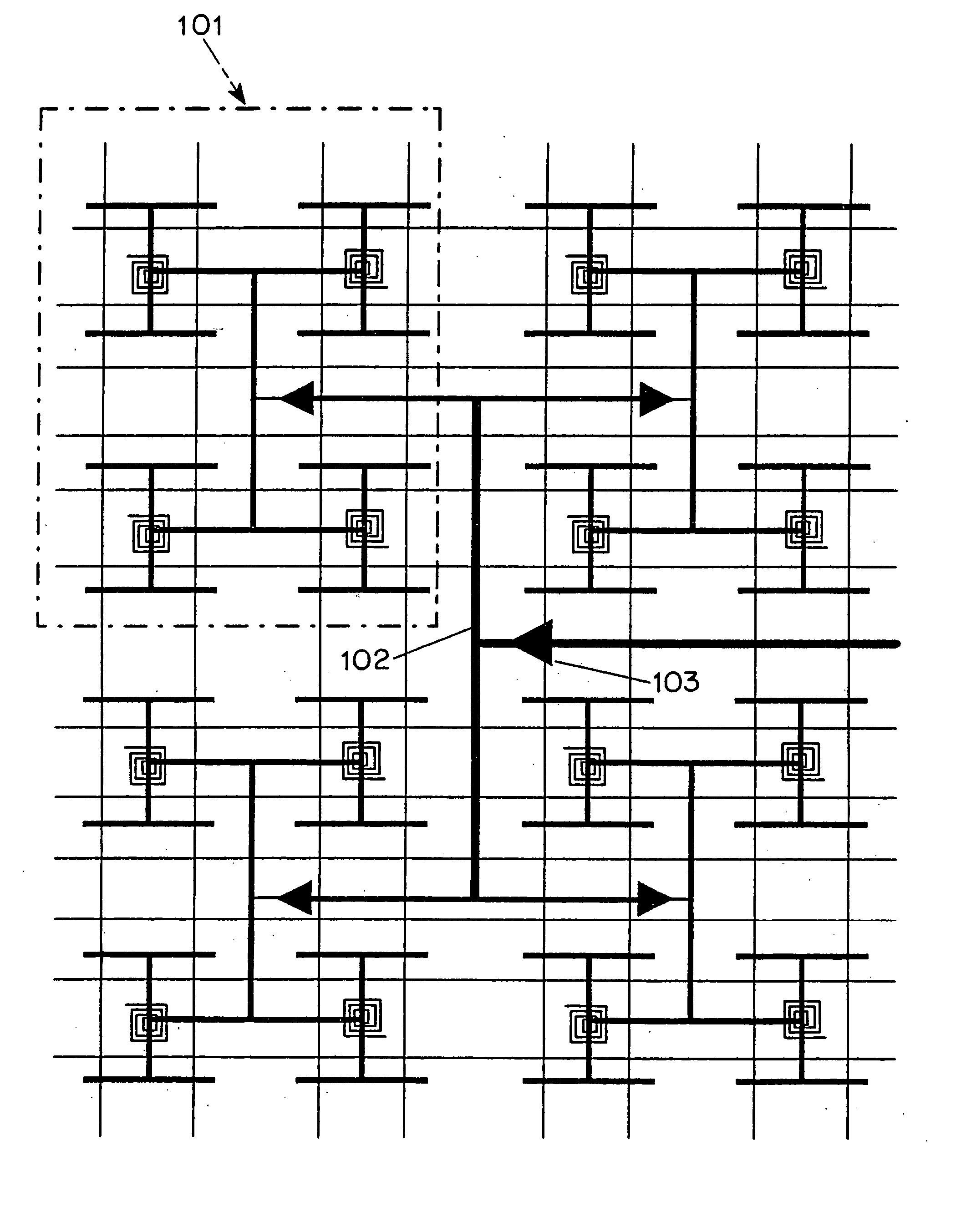
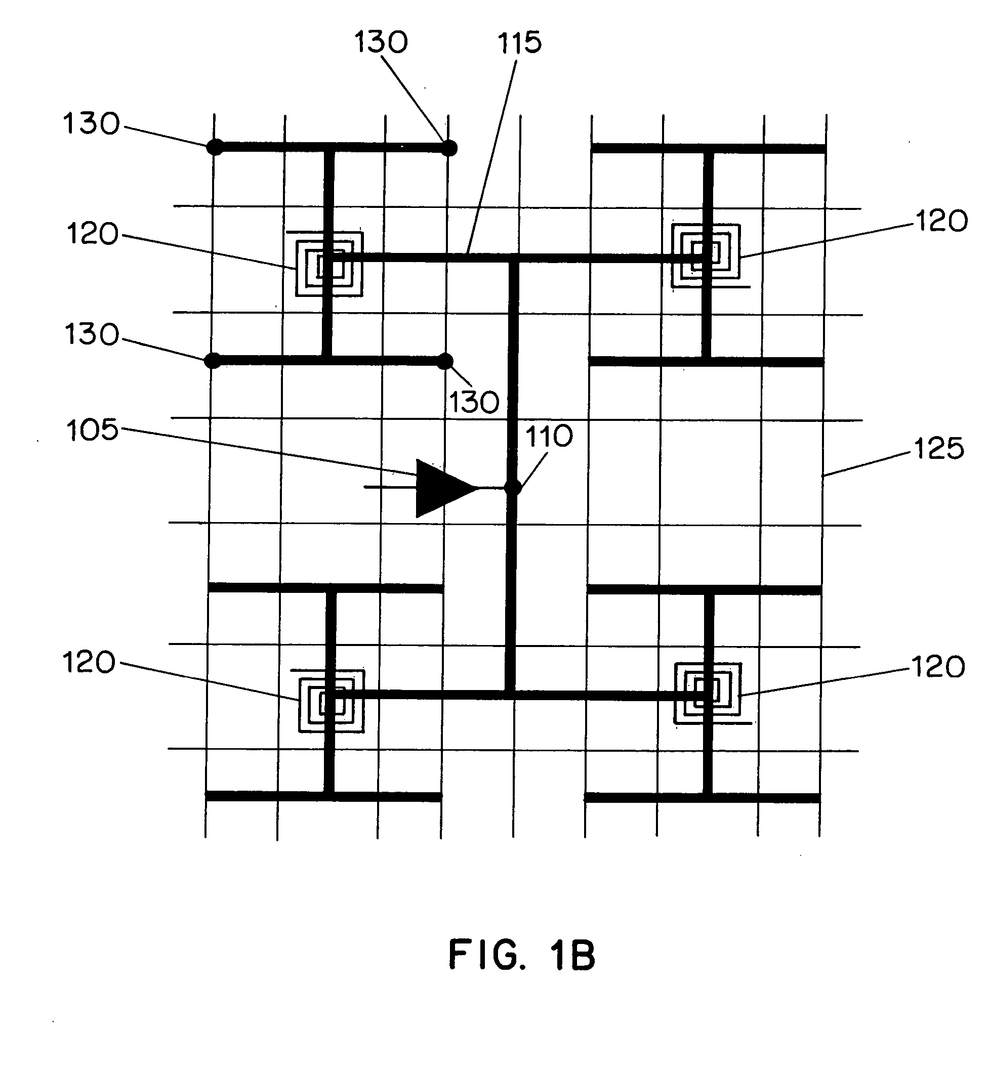
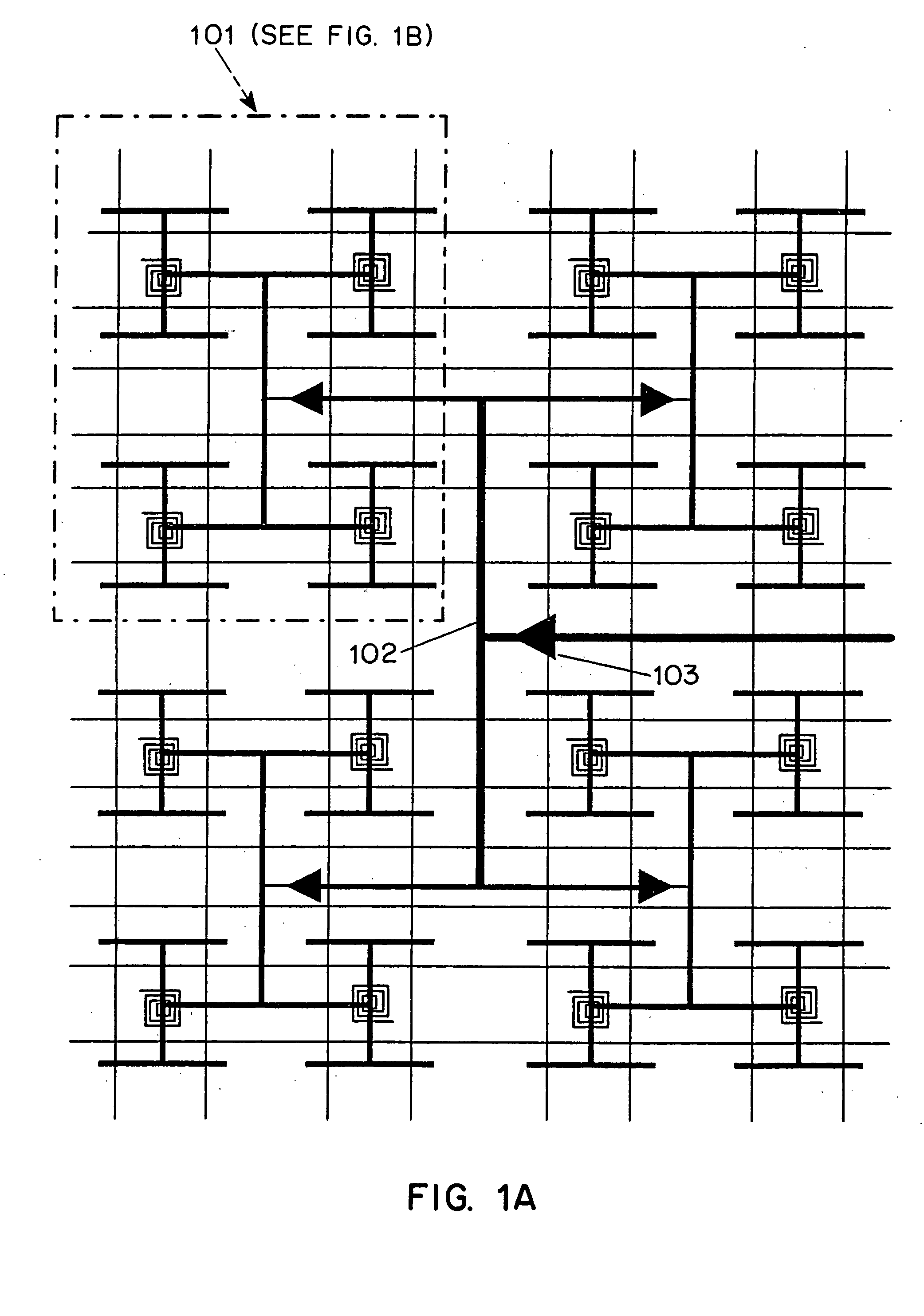
[0033]FIG. 1A is pictorial diagrams illustrating a top planar view of an embodiment of the present resonant clock distribution circuit as viewed through a number of metalization layers of an integrated circuit. The circuit of FIG. 1B illustrates a single sector 101 of the circuit of FIG. 1A. The circuit of FIG. 1B may represent a sector having an area of about 2,500 μM×2,500 μM. A typical microprocessor clock distribution may include several dozen of such clock distribution sectors, which are coupled together to provide a global clock distribution circuit. The circuit of FIG. 1A illustrates the circuit of FIG. 1B implemented in four adjacent sectors of an integ...


PUM


Abstract

A circuit for distributing a clock signal in an integrated circuit includes a capacitive clock distribution circuit having at least conductor therein. At least one inductor is formed in a metal layer of the integrated circuit and is coupled to the clock distribution circuit. The inductor, generally in the form of a number of spiral inductors distributed throughout the integrated circuit, provides an inductance value selected to resonate with the capacitive clock distribution circuit. By operating the clock distribution circuit at resonance, power dissipation is reduced while skew and jitter performance can be improved.

Description

CROSS-REFERENCE TO PRIORITY AND RELATED APPLICATION [0001] This application claims the benefit of U.S. provisional patent application Ser. No. 60 / 490,063 filed on Jul. 24, 2003, and is a continuation-in-part of U.S. patent application Ser. No. ______ filed on Jul. 9, 2004 in the U.S. national stage of International application No. PCT / US03 / 00932, all of which applications are incorporated by reference in their entireties herein.FIELD OF THE INVENTION [0002] The present invention relates generally to clock distribution in integrated circuits and more particularly relates to methods of distributing a high frequency clock with improved power efficiency and skew and jitter performance. BACKGROUND OF THE INVENTION [0003] Clocking large digital chips with a single high-frequency global clock is becoming an increasingly difficult task. As circuit size and clock frequency continue to increase, skew and jitter as well as power consumption are becoming increasingly important design considerat...

Claims


Application Information

Patent Timeline
Patent Type & Authority Applications(United States)
IPC IPC(8): G06F1/10H03L7/00
CPCG06F1/10
Inventor SHEPARD, KENCHAN, STEVEN
Owner THE TRUSTEES OF COLUMBIA UNIV IN THE CITY OF NEW YORK
Why Eureka
Try Eureka