Method and apparatus for providing parallel optoelectronic communication with an electronic device

a technology of optoelectronic communication and electronic devices, applied in the direction of optical waveguide light guide, instruments, optics, etc., can solve the problems of signal loss and distortion in the electrical transport media, the inability to scale to the bandwidth/distance requirements of next-generation servers, and the use of copper interconnect technology as the interconnect medium

Active Publication Date: 2005-03-17
IBM CORP
View PDF9 Cites 59 Cited by
  • Summary
  • Abstract
  • Description
  • Claims
  • Application Information

AI Technical Summary

Problems solved by technology

To connect between multiple MCMs, copper interconnect technology has been used as the interconnect medium, but is limited in its ability to scale to the bandwidth/distance requirements of next generation servers.
These limitations are primarily associated with the signal loss and distortion in the electrical transport media, su

Method used


Image

  • Method and apparatus for providing parallel optoelectronic communication with an electronic device
  • Method and apparatus for providing parallel optoelectronic communication with an electronic device
  • Method and apparatus for providing parallel optoelectronic communication with an electronic device

Examples


Embodiment Construction

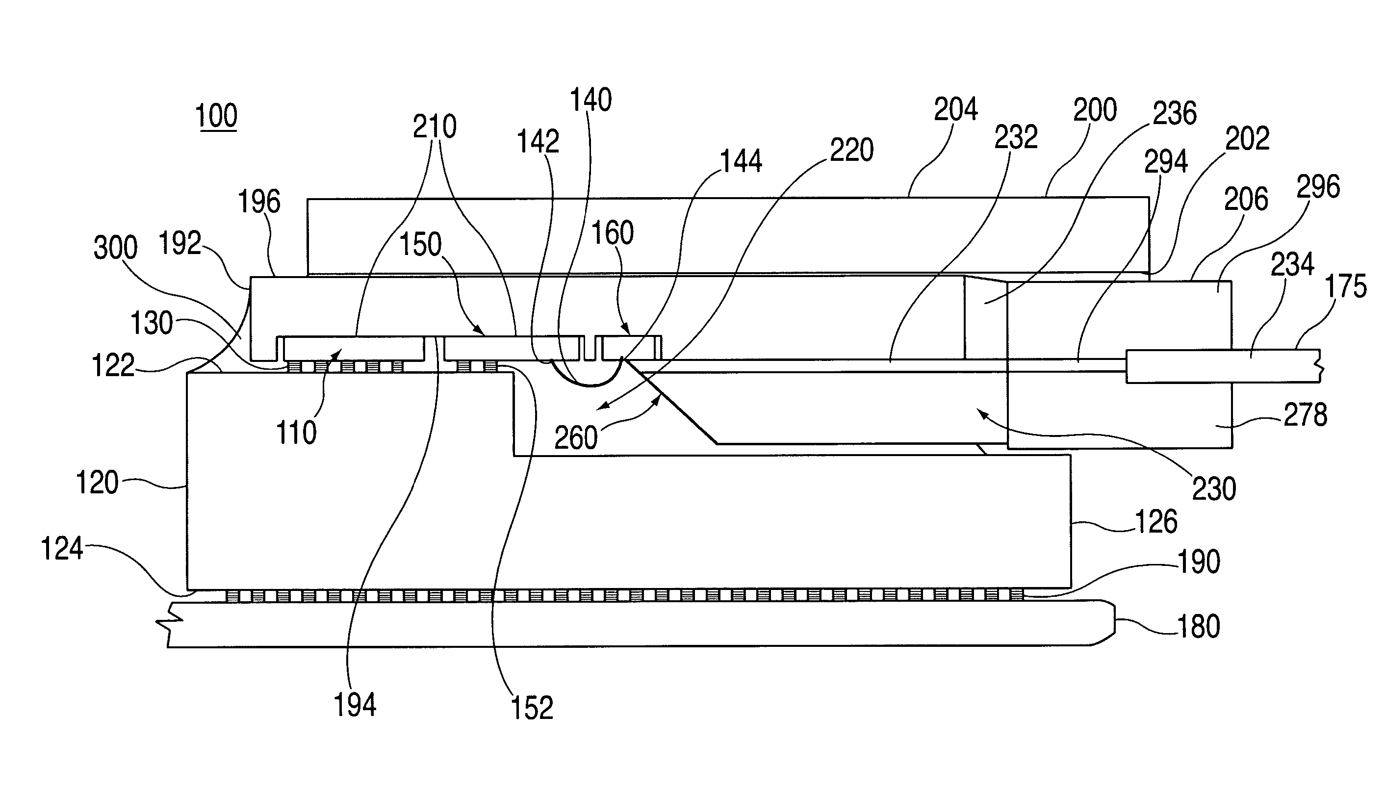
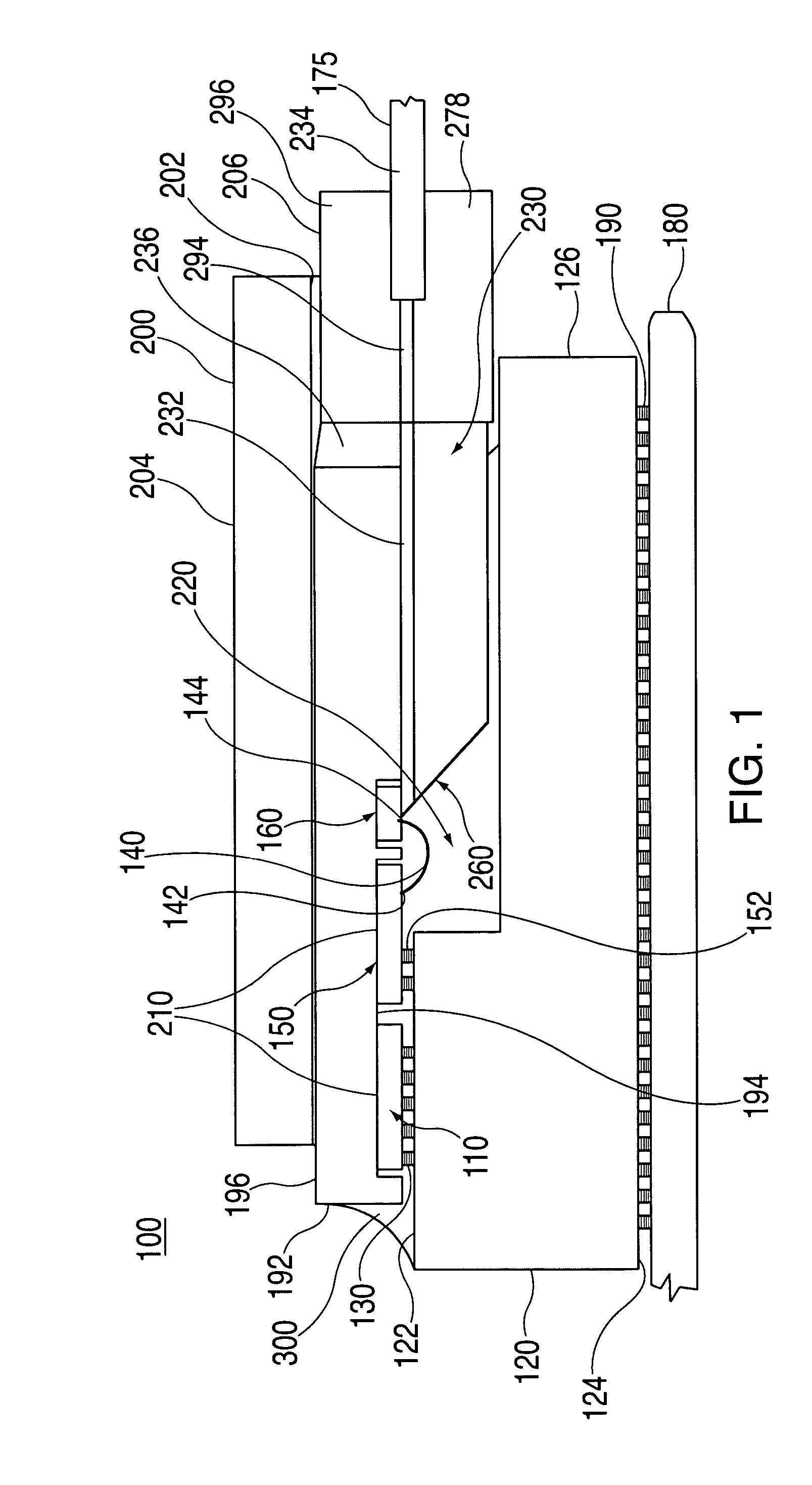
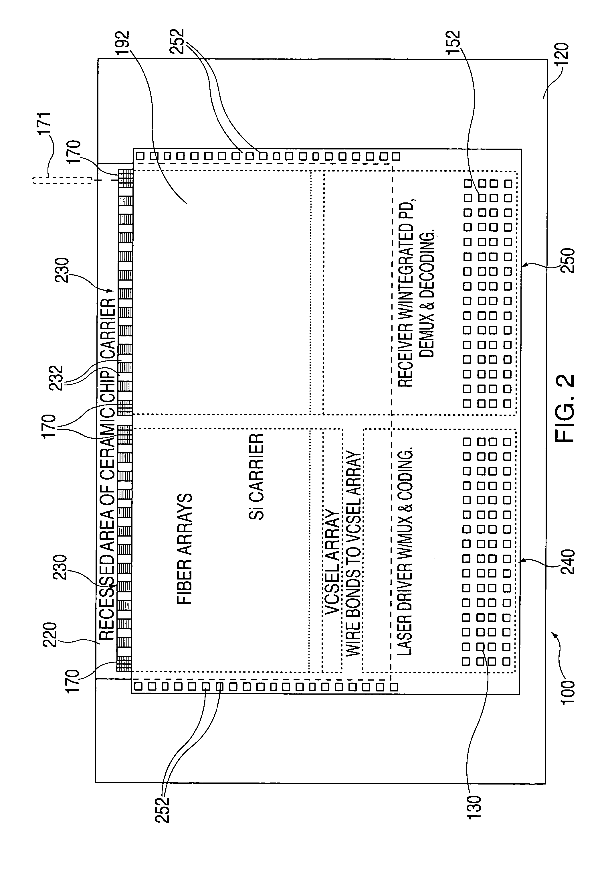
[0014] An embodiment of the present invention provides an optoelectronic assembly which can be mounted on a first level package, such as an MCM, using C4, or micro solder balls (less than or equal to 500 micrometer pitch), just as the chips are attached, for a computer system, data communication system, or other electronic system, having a data communication path between an electronic computer, signal processing chip or other electronic chip, and an optoelectronic transducer that bypasses a printed circuit board, or other second level package, thereby providing high speed communication from the electronic chip to other components in the computer system, switching system or other electronic system. Another embodiment provides a high density optical signal path by using multiple optoelectronic transducers, alternatively referred to as a high density optical transceiver (HDOT). While embodiments described herein depict the interconnection of a processor complex within a Multi-Chip Modu...


PUM


Abstract

An optoelectronic assembly for an electronic system includes a support electronic chip set configured for at least one of providing multiplexing, demultiplexing, coding, decoding and optoelectronic transducer driving and receive functions. A first substrate having a first surface and an opposite second surface is in communication with the support electronic chip set via the first surface while a second substrate is in communication with the second surface of the first substrate. The second substrate is configured for mounting at least one of data processing, data switching and data storage chips. An optoelectronic transducer is in signal communication with the support electronic chip set and an optical fiber array is aligned at a first end with the optoelectronic transducer and with an optical signaling medium at a second end. An electrical signal from the support electronic chip set is communicated to the optoelectronic transducer via an electrical signaling medium, and the support electronic chip set and the optoelectronic transducer share a common thermal path for cooling.

Description

BACKGROUND OF THE INVENTION [0001] The present disclosure relates generally to optoelectronic communication with an electronic device, and particularly to the attachment arrangement for providing parallel optoelectronic communication between an electronic chip on a first level package to another electronic chip on another first level package using a high density optical transceiver. [0002] Typically, optoelectronic transceivers are mounted on a second level package, such as a printed circuit board, and are provided with their own heat sink and a means of being electrically interconnected with a printed circuit board, such as via a socket or a solder Ball Grid Array (BGA). The typical pitch of the electrical connections in a BGA is approximately 1.27 mm, although some products use finer pitches such as 1.0 or 0.8 mm. The size of an optoelectronic transceiver is largely determined by the area required by the heat sink and / or the area required for electrical connections between the opt...

Claims


Application Information

Patent Timeline
IPC IPC(8): G02B6/42
CPCG02B6/4214G02B6/4249G02B6/4246
Inventor COLGAN, EVAN G.FURMAN, BRUCE K.STIGLIANI, DANIEL J. JR.
Owner IBM CORP
Why Eureka
Try Eureka