

Wafer edge inspection data gathering
a technology of wafer edge and data gathering, which is applied in the direction of mechanical roughness/irregularity measurement, semiconductor/solid-state device testing/measurement, instruments, etc., can solve the problems of too time-consuming and unreliable to adequately address the problem of wafer edge defects, and achieve the effect of efficient operation, quick location or identification
- Summary
- Abstract
- Description
- Claims
- Application Information
AI Technical Summary
Benefits of technology
Problems solved by technology
Method used
Image

Examples
Embodiment Construction
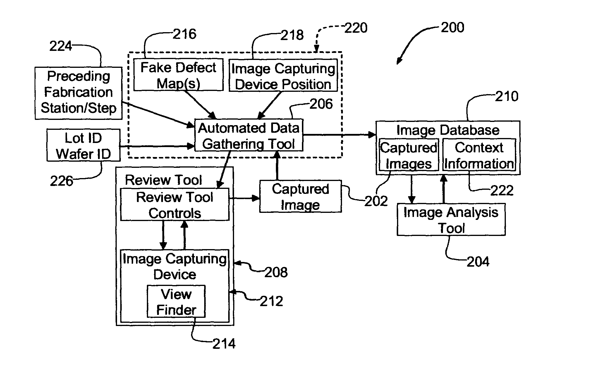
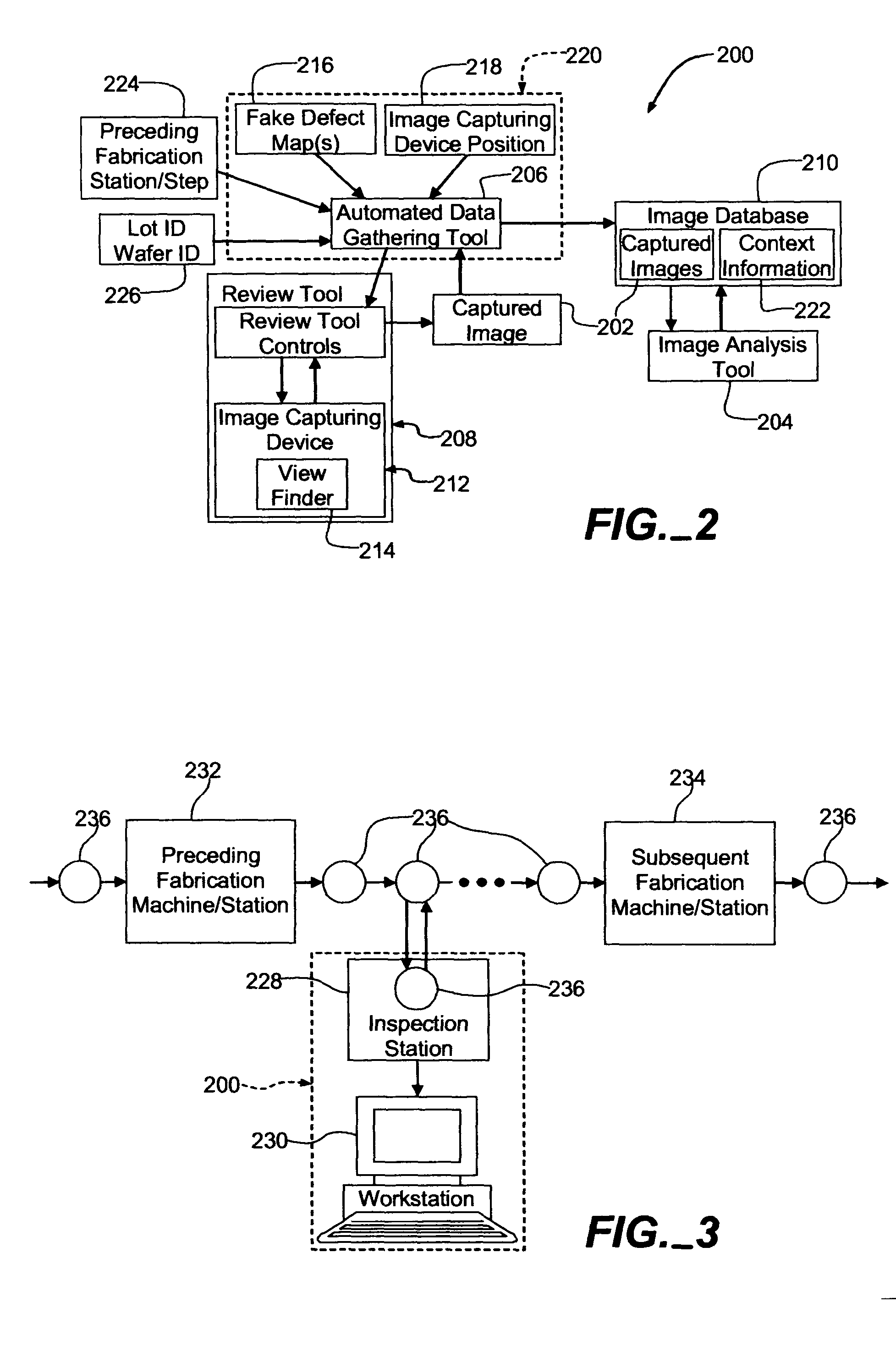
[0025] An exemplary wafer edge inspection system 200, as shown in FIG. 2, generally captures images 202 of the edge of a wafer (not shown), such as a semiconductor wafer used in the fabrication of integrated circuits, for detailed computer analysis thereof by an image analysis tool 204. The image analysis tool 204 generally analyzes the captured images 202 as described in the aforementioned patent application.
[0026] In addition to the image analysis tool 204, the wafer edge inspection system 200 generally includes an automated data gathering tool 206, a conventional review tool 208 and an image database 210. The automated data gathering tool 206, the review tool 208 and the image database 210 generally function together to automate the data capture, storage and management for the wafer edge inspection system 200.
[0027] The review tool 208 generally includes wafer inspection hardware, such as an image capturing device 212 having a view finder 214. The review tool 208 generally rece...
PUM
| Property | Measurement | Unit |
|---|---|---|
| Edge Defect Inspection | aaaaa | aaaaa |
| yield rate | aaaaa | aaaaa |
| size | aaaaa | aaaaa |
Abstract
Description
Claims
Application Information