Fabrication method of semiconductor integrated circuit device

a technology of integrated circuit devices and manufacturing methods, which is applied in the direction of semiconductor/solid-state device details, manufacturing tools, solid-state devices, etc., can solve the problems of imperfect bonding, difficulty in disposing a heating mechanism above the wiring substrate, and insufficient rise of the bonding portions

Inactive Publication Date: 2005-03-24
RENESAS ELECTRONICS CORP +1
View PDF7 Cites 55 Cited by
  • Summary
  • Abstract
  • Description
  • Claims
  • Application Information

AI Technical Summary

Benefits of technology

[0009] To effect bonding between a wiring substrate and semiconductor chips by flip-chip connection, the semiconductor chips are picked up from a semiconductor wafer; then they are disposed o

Problems solved by technology

On the other hand, it is difficult to dispose a heating mechanism above the wiring substrate because of the fact that the conveyance mechanism is disposed above the substrate, and, therefore, the heating mechanism typically is embedded into a stage located below the wiring substrate.
In this structure, if heating is conducted from the stage side, the chip-substrate bonding portions are heated through the wiring su

Method used


Image

  • Fabrication method of semiconductor integrated circuit device
  • Fabrication method of semiconductor integrated circuit device
  • Fabrication method of semiconductor integrated circuit device

Examples


embodiments

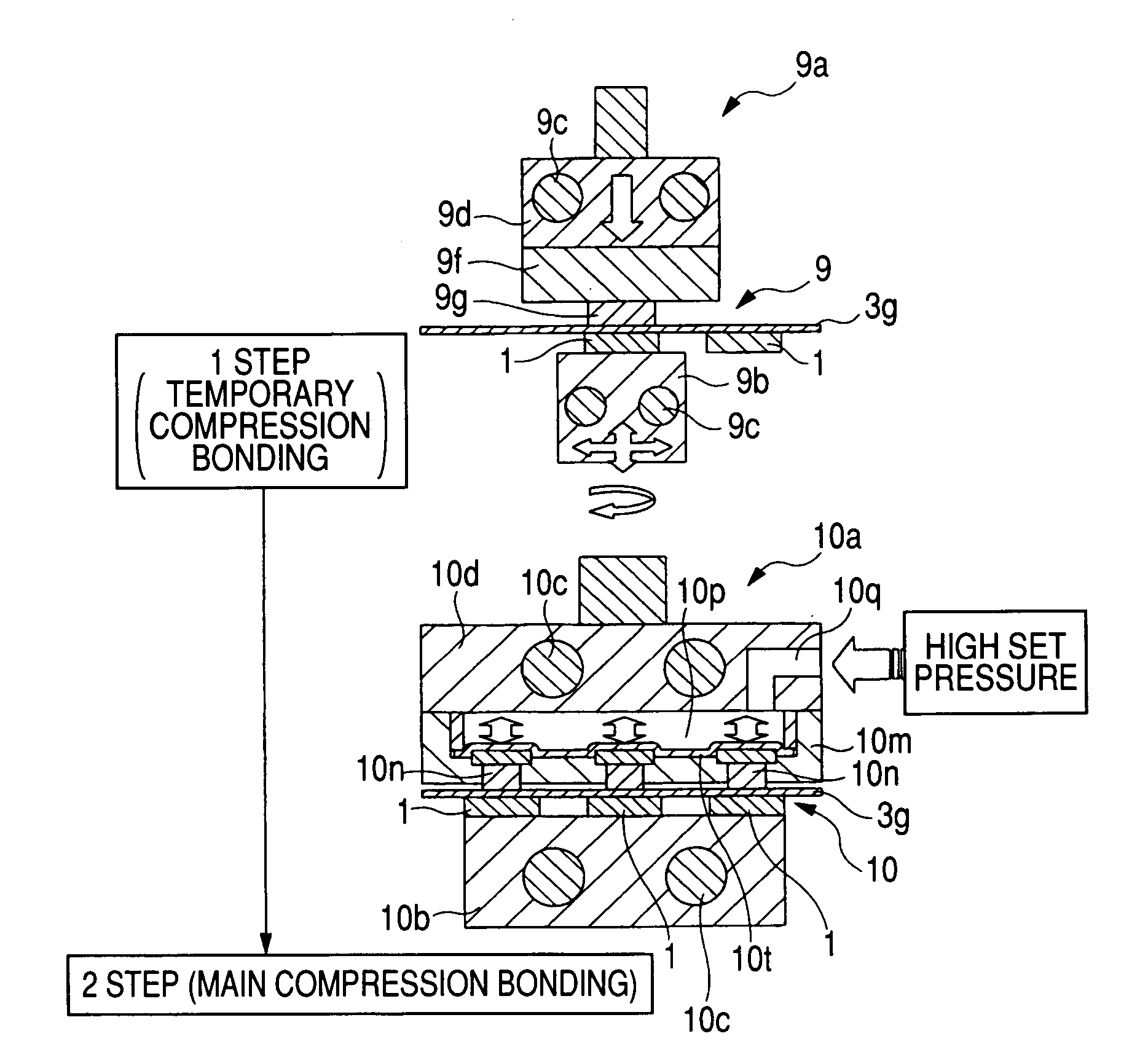
[0121] (Embodiments)

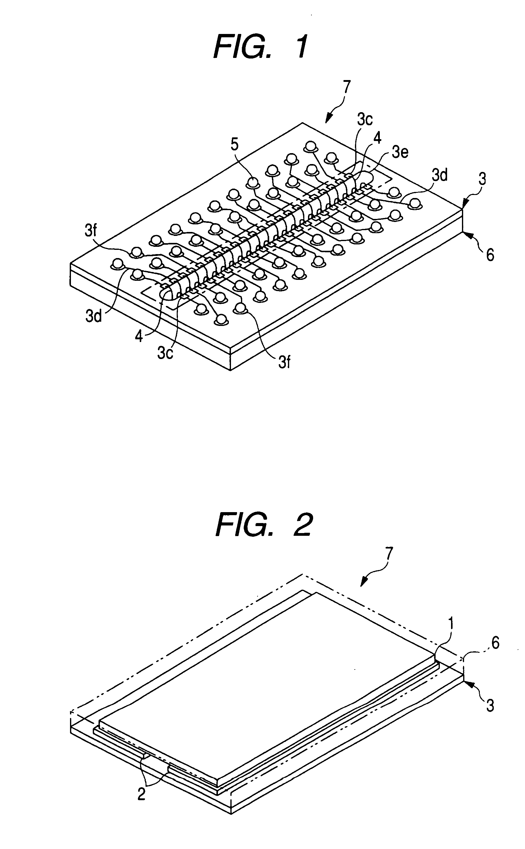
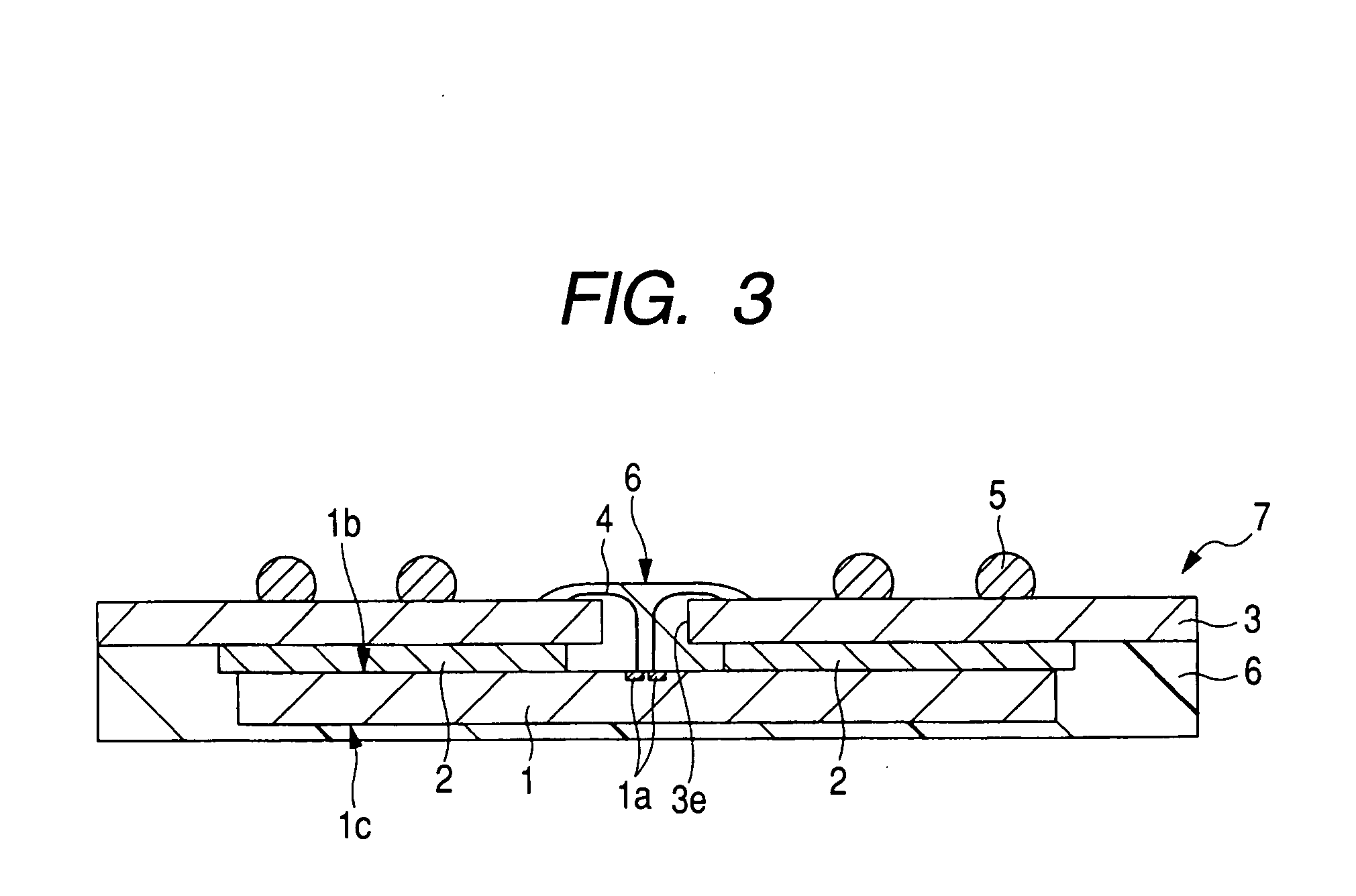
[0122] A semiconductor integrated circuit device embodying the present invention is in the form of a resin-sealed semiconductor package wherein an organic substrate 3 serving as a wiring substrate and a semiconductor chip 1 are bonded together. In this embodiment, reference will be made as an example to a BOC (Board On Chip) 7, as shown in FIG. 1.

[0123] A description will now be given of the structure of the BOC 7 shown in FIGS. 1 to 3. The BOC 7 comprises an organic substrate 3. The organic substrate 3 has an elongated aperture 3e formed centrally and longitudinally of one face of the organic substrate. Bump lands 3f are formed in two rows on each of both sides of the aperture 3e, plural bonding electrodes 3c are formed in proximity to the aperture 3e, and wires 3d are provided for connecting the bump lands 3f and the bonding electrodes 3c electrically with each other.

[0124] A semiconductor chip 1 is bonded to the opposite face of the organic substrate 3 throu...


PUM

PropertyMeasurementUnit
Temperatureaaaaaaaaaa

Abstract

Productivity is to be improved in assembling a semiconductor integrated circuit device. A matrix substrate is provided and semiconductor chips are disposed on a first heating stage, and then the matrix substrate is disposed above the semiconductor chips on the first heating stage. Subsequently, the semiconductor chips and the matrix substrate are bonded to each other temporarily by thermocompression bonding, while heating the chips directly by the first heating stage. Thereafter, the temporarily bonded matrix substrate is disposed on a second heating stage adjacent to the first heating stage, and then, on the second heating stages, the semiconductor chips are thermocompression-bonded to the matrix substrate, while being heated directly by the second heating stage.

Description

CROSS-REFERENCE TO RELATED APPLICATION [0001] The present application claims priority from Japanese Patent application JP 2003-327046, filed on Sep. 19, 2003, the content of which is hereby incorporated by reference into this application. BACKGROUND OF THE INVENTION [0002] The present invention relates to a method of fabricating a semiconductor integrated circuit device, and, more particularly, to a technique for use in the fabrication of a semiconductor integrated circuit device wherein a semiconductor chip is bonded to a substrate. [0003] In the conventional way of providing bonding between a substrate and silicon chips, the substrate is disposed on a substrate rest (stage); then, plural silicon chips are arranged on the substrate; and heat is conducted to the silicon chips through the substrate by means of a heating cartridge provided on the substrate rest (see, for example, Patent Literature 1 and Patent Literature 2, which is a European patent application corresponding to Paten...

Claims


Application Information

Patent Timeline
IPC IPC(8): H01L21/60B23K31/02H01L21/50H01L21/52H01L21/56H01L21/58H01L23/31
CPCH01L21/561H01L2924/10253H01L24/83H01L24/97H01L2224/48091H01L2224/4824H01L2224/48247H01L2224/4826H01L2224/73215H01L2224/83101H01L2224/83192H01L2224/8385H01L2224/92147H01L2224/97H01L2924/01005H01L2924/01015H01L2924/01029H01L2924/01033H01L2924/01057H01L2924/01079H01L2924/01082H01L2924/07802H01L2924/10329H01L2924/12044H01L2924/14H01L2924/15311H01L23/3128H01L2224/32225H01L2224/45147H01L2224/45144H01L2924/0132H01L2924/0665H01L2924/014H01L2924/01006H01L2224/2919H01L24/48H01L24/29H01L2224/85H01L2224/83H01L2924/00014H01L2924/00H01L2924/01031H01L2924/00012H01L24/75H01L24/45H01L2924/181H01L2224/32245H01L2224/05599H01L21/52
Inventor MAKI, HIROSHITANI, YUKIO
Owner RENESAS ELECTRONICS CORP
Why Eureka
Try Eureka