Nonvolatile semiconductor memory device and manufacturing method thereof

a semiconductor memory and non-volatile technology, applied in the direction of digital storage, instruments, transistors, etc., can solve the problems of increasing the thickness of the insulator film electrically isolating the two gate electrodes constituting the split gate, and the unignorable size of the data-line pitch by this method, so as to reduce the electrical resistance of the diffusion layer, reduce the punch, and ensure the effect of reading speed

Inactive Publication Date: 2005-03-24
RENESAS TECH CORP
View PDF6 Cites 16 Cited by
  • Summary
  • Abstract
  • Description
  • Claims
  • Application Information

AI Technical Summary

Benefits of technology

[0008] In the flash memory having a so-called AND array structure, when the data-line pitch in all the memory cells is reduced, there arise in common two problems of: 1) ensuring a reading speed by reducing electrical resistance of the diffusion layer or the inversion layer which constitutes the data line; and 2) reducing punch through due to the short-channel effect by ensuring an channel length between the source and drain, and it is required to simultaneously achieve the two problems.

Problems solved by technology

In the flash memory having a so-called AND array structure, when the data-line pitch in all the memory cells is reduced, there arise in common two problems of: 1) ensuring a reading speed by reducing electrical resistance of the diffusion layer or the inversion layer which constitutes the data line; and 2) reducing punch through due to the short-channel effect by ensuring an channel length between the source and drain, and it is required to simultaneously achieve the two problems.
Similarly, in the split-gate flash memory having an NOR array structure, when the source-line pitch in all the memory cells is reduced, there arise in common two problems of: 1) ensuring a reading speed by reducing the resistance of the source lines; and 2) suppressing the punch through due to the short-channel effect by ensuring the channel length between the source and drain, and it is required to simultaneously achieve the two problems.
However, when the data-line pitch is further reduced, the thickness of an insulator film electrically isolating two gate electrodes constituting the split gate, that is, the floating gate and the assist gate, becomes unignorable large relative to the data-line pitch.
Therefore, there is a possibility that the reduction of the data-line pitch by this method will reach a limit.
Meanwhile, in another cell method (Patent Document 3) in which the inversion layer is used as the data line, since the resistance of the inversion layer is larger than that of the diffusion layer, there is the problem that the readout performance particularly degrades.

Method used


Image

  • Nonvolatile semiconductor memory device and manufacturing method thereof
  • Nonvolatile semiconductor memory device and manufacturing method thereof
  • Nonvolatile semiconductor memory device and manufacturing method thereof

Examples


first embodiment

[0067] (First Embodiment)

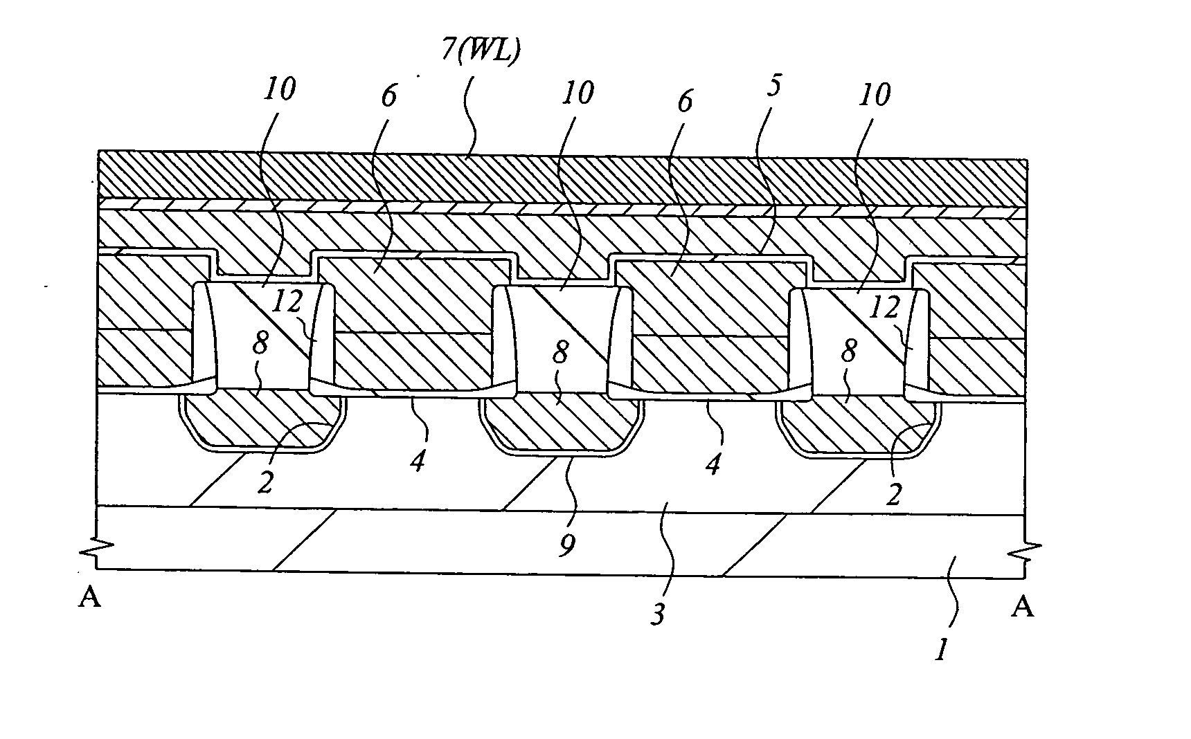
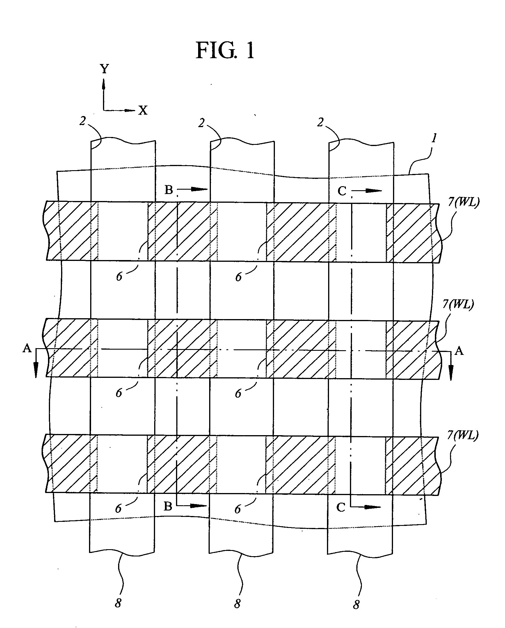
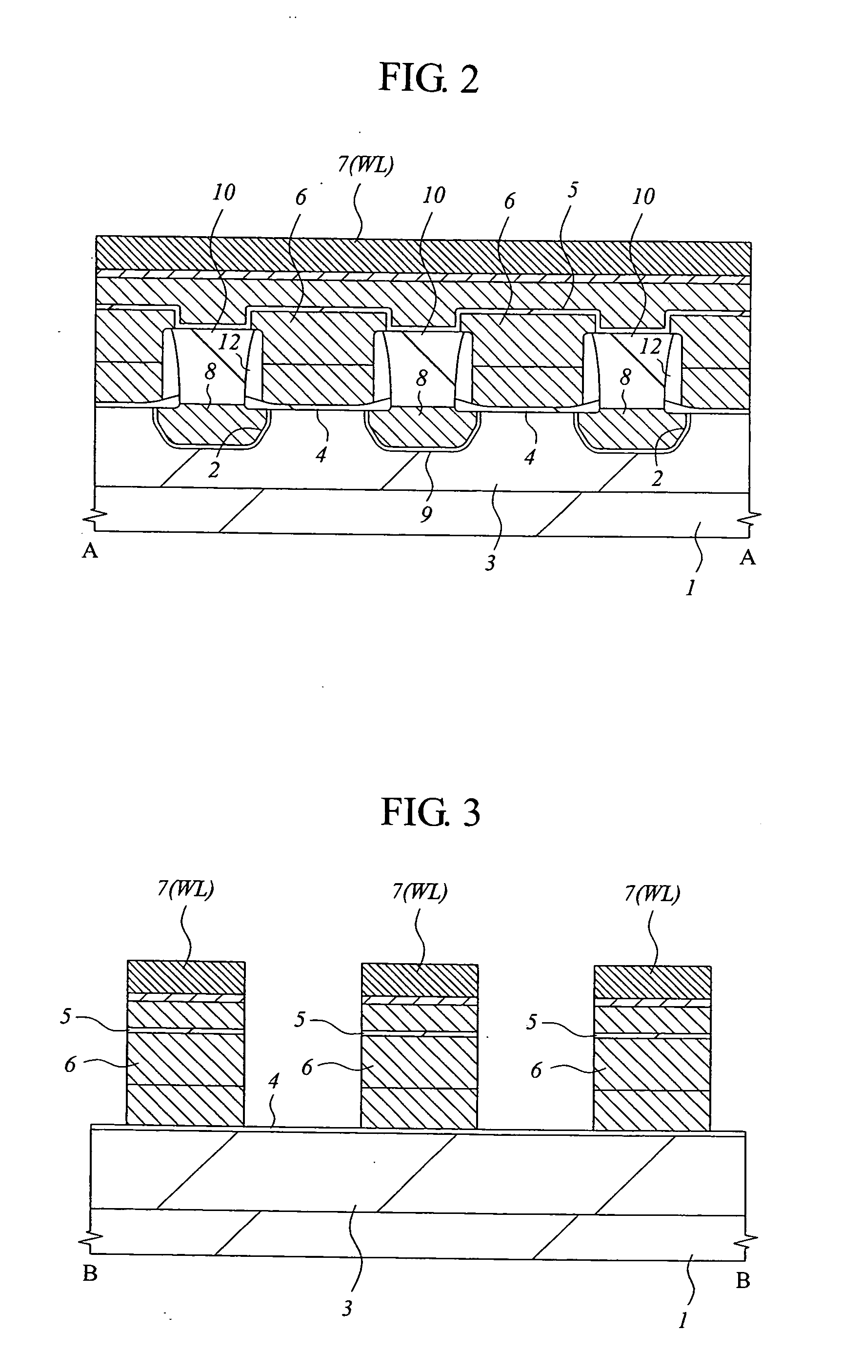
[0068]FIG. 1 is a plan view showing the principal part of a memory array structure of a semiconductor memory device according to a first embodiment of the present invention; FIG. 2 is a sectional view showing the principal part of a semiconductor substrate taken along the line A-A in FIG. 1; FIG. 3 is a sectional view showing the principal part of a semiconductor substrate taken along the line B-B inFIG. 1; and FIG. 4 is a sectional view showing the principal part of a semiconductor substrate taken along the line C-C in FIG. 1. Note that some components such as an insulator film are omitted in FIG. 1 (plan view) in order to make the drawing easy to see.

[0069] A semiconductor memory device according to this embodiment is a so-called flash memory, and has a memory array in which a plurality memory cells are formed in and on a p type well 3 disposed on a main surface of a semiconductor substrate (hereinafter “substrate”) 1 made of single crystal silicon. Each ...

second embodiment

[0094] (Second Embodiment)

[0095] In the first embodiment, the inversion layer formed by applying the positive voltage to the buried gate (third gate electrode) 8 is used as the data line. However, it is also possible to further provide a diffusion layer 20 in the substrate 1 (p type well 3) disposed below the buried gate (third gate electrode) 8, as shown in FIGS. 21 and 22.

[0096] The diffusion layer 20 is formed in the following manner. First, as shown in FIG. 23, the patterns (P) composed of a stacked film of the silicon nitride film 11 and the polysilicon film 6a are formed over the substrate 1 (p type well 3) via the first gate insulator film 4, and then the sidewall spacers 12 are formed on the sidewalls of the patterns (P). Thereafter, the grooves 2 are formed in the substrate 1 disposed below the space regions between the patterns (P). The process until then is identical to that in the first embodiment shown in FIGS. 7 to 11.

[0097] Next, as shown in FIG. 24, an n type impur...

third embodiment

[0101] (Third Embodiment)

[0102] In the second embodiment, the diffusion layer 20 is provided below all of the buried gates 8 formed in the memory array. However, the diffusion layer 20 may be provided only below the predetermined buried gates 8, as shown in FIG. 27.

[0103] In this case, as shown in FIG. 28, a photoresist film 30 is formed to cover the groove 2 in which the diffusion layer 20 is not formed when an n type impurity is ion-implanted into the substrate 1 in the process as shown in FIG. 23 in the second embodiment.

[0104] The operation of the memory cell will be described with reference to FIGS. 29 and 30. In the reading operation, as shown in FIG. 29, of the buried gates 8 on both sides of the selected memory cell, a voltage of about 5 V is applied to the buried gate 8 not having the diffusion layer 20, and a voltage of about 1 V is applied to the inversion layer thereof. Also, a voltage of about 3 V is applied to the buried gate 8 having the diffusion layer 20, and the ...


PUM


Abstract

A nonvolatile semiconductor memory device, in which an inversion layer formed over a semiconductor substrate is used as a data line, is achieved with its high integration and high performance. A memory cell is composed of a MOS transistor having a floating gate, a control gate constituting a word line, and a buried gate. The buried gate is buried in a groove formed in a self-alignment manner with respect to the floating gate. The buried gate and the control gate disposed over it are isolated from each other by a thick silicon oxide film on the groove and a second gate insulator film formed thereon. A source and drain of the memory cell are composed of an inversion layer (local data line) formed on a p type well disposed below the buried gate when a positive voltage is applied to the buried gate.

Description

CROSS-REFERENCE TO RELATED APPLICATION [0001] The present application claims priority from Japanese patent application No. JP 2003-331546 filed on Sep. 24, 2003, the content of which is hereby incorporated by reference into this application. BACKGROUND OF THE INVENTION [0002] The present invention relates to a nonvolatile semiconductor memory device and a manufacturing method thereof. More particularly, the present invention relates to a technique effectively applied to achieve higher integration and higher performance of an electrically rewritable nonvolatile semiconductor memory device. [0003] As an electrically rewritable nonvolatile semiconductor memory device which can perform a bulk erase of data, a so-called flash memory is well known. Since the flash memory is excellent in portability and shock resistance and can be electrically bulk erased, the demands for the flash memory as a memory device for mobile information appliances such as a portable personal computer and a digita...

Claims


Application Information

Patent Timeline
Patent Type & Authority Applications(United States)
IPC IPC(8): G11C16/04H01L21/8247H01L27/115H01L29/423H01L29/788H01L29/792
CPCG11C16/0433G11C16/0491H01L29/42336H01L27/11521H01L29/42328H01L27/115H10B69/00H10B41/30
Inventor SASAGO, YOSHITAKAKOBAYASHI, TAKASHI
Owner RENESAS TECH CORP
Why Eureka
Try Eureka