Quantum efficiency enhancement for CMOS imaging sensor with borderless contact

a cmos imaging sensor and quantum efficiency technology, applied in the field of fabrication of image sensors, can solve the problems of loss, destructive interference, and still be found in the structure of destructive interference, and achieve the effect of high quantum efficiency

Inactive Publication Date: 2005-03-24
TSMC CHINA COMPANY
View PDF33 Cites 12 Cited by
  • Summary
  • Abstract
  • Description
  • Claims
  • Application Information

AI Technical Summary

Benefits of technology

Accordingly, it is a primary object of the present invention to provide a high quantum efficiency image sensor.

Problems solved by technology

All of the light that passes through the internal structure of the detector should be absorbed, but losses can occur due to light reflection or destructive interference.
This destructive interference is caused by the presence of the silicon oxynitride layer.
The destructive interference will still be found in this structure.

Method used


Image

  • Quantum efficiency enhancement for CMOS imaging sensor with borderless contact
  • Quantum efficiency enhancement for CMOS imaging sensor with borderless contact
  • Quantum efficiency enhancement for CMOS imaging sensor with borderless contact

Examples


Embodiment Construction

The present invention provides a method of fabricating a high performance CMOS photodiode, made with or without borderless contact processes, having enhanced quantum efficiency, and a corresponding structure of an image sensor having a photodiode having enhanced quantum efficiency.

The enhanced quantum efficiency of the photodiode of the present invention is achieved by the introduction of a layer between the ILD and the silicon photodiode having a refraction index in between the high rate of the silicon and the low rate of the ILD layer.

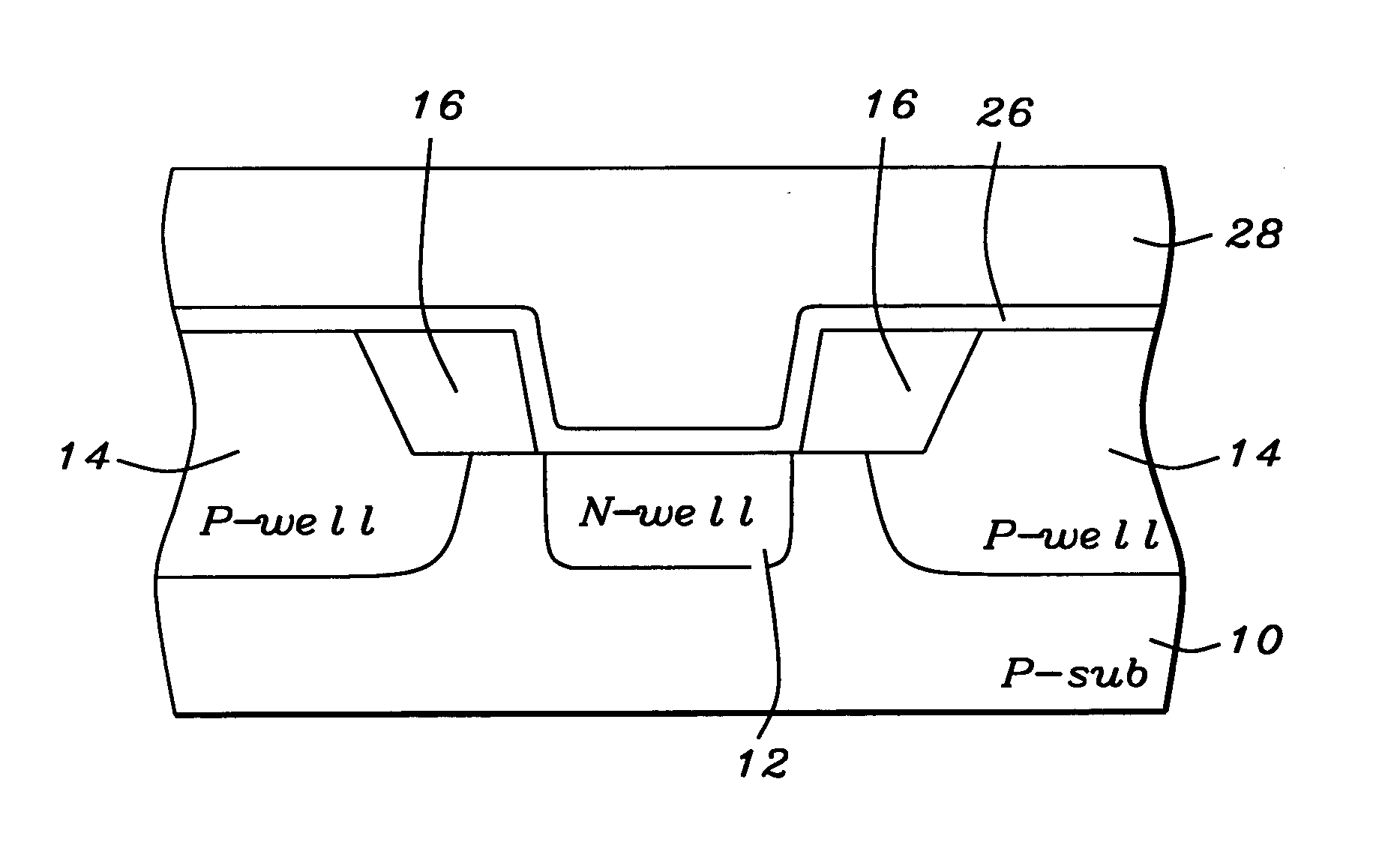
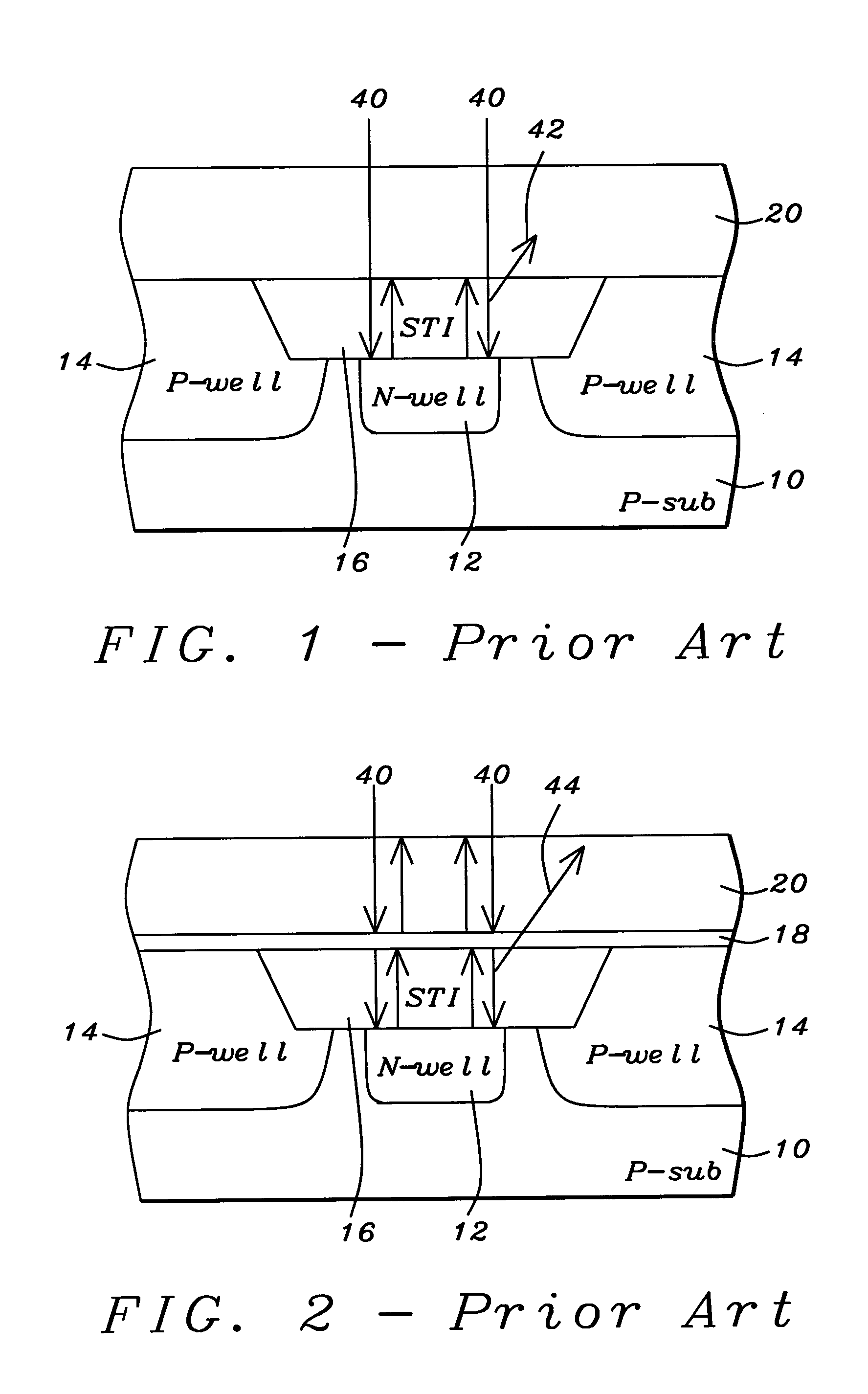
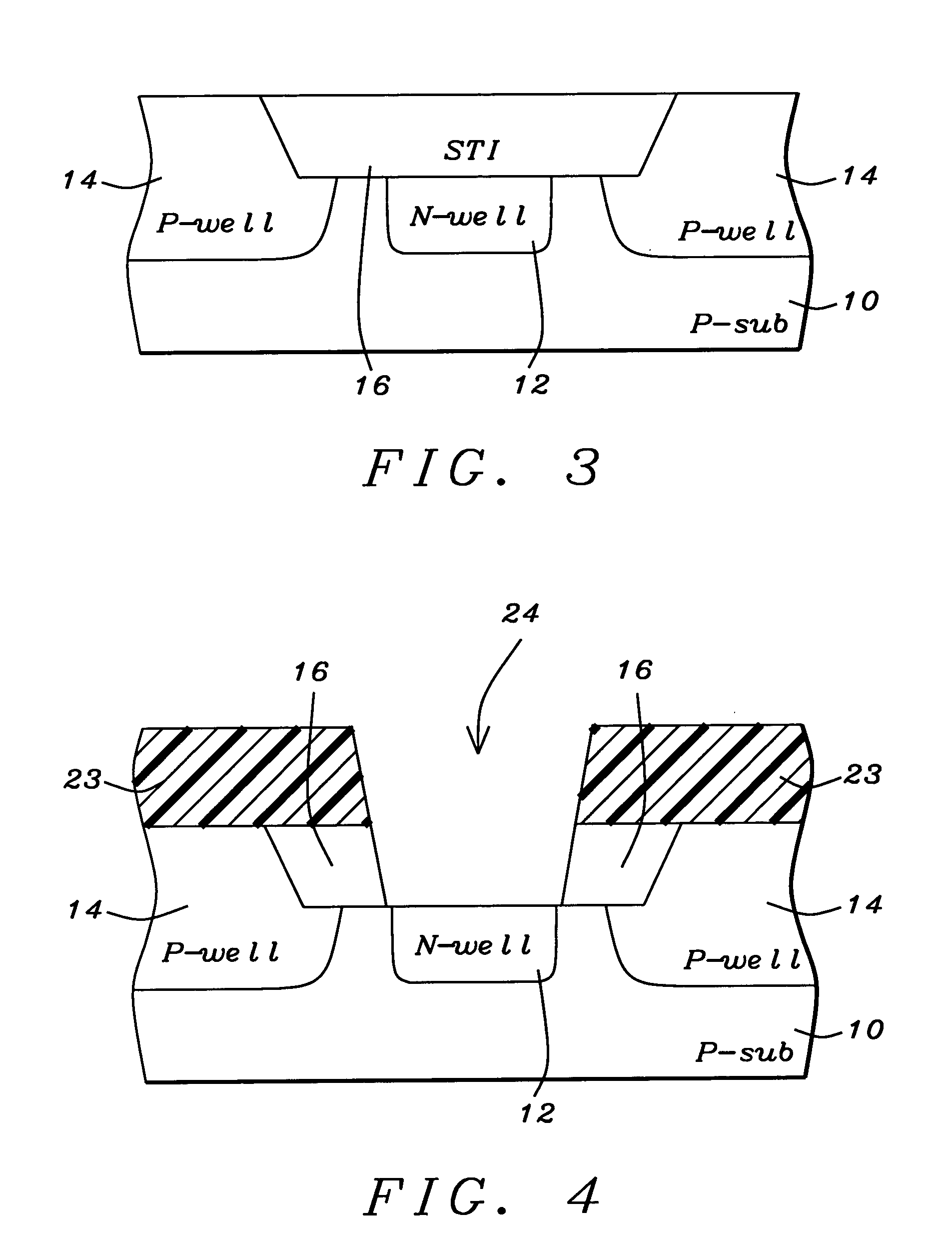
The process of the present invention will be described with reference to FIGS. 3-6. An N-type photosensor is illustrated in the drawings, but it will be understood by those skilled in the art that a P-type photosensor may be formed by reversing the conductivity of the substrate and well regions. Referring now more particularly to FIG. 3, there is shown p-doped silicon substrate 10. P-wells 14 have been formed in the substrate. A Shallow Trench I...


PUM


Abstract

The present invention is a CMOS image sensor and its method of fabrication. This invention provides an efficient structure to improve the quantum efficiency of a CMOS image sensor with borderless contact. The image sensor comprises a N-well/P-substrate type photodiode with borderless contact and dielectric structure covering the photodiode region. The dielectric structure is located between the photodiode and the interlevel dielectric (ILD) and is used as a buffer layer for the borderless contact. The method of fabricating a high performance photodiode comprises forming a photodiode in the n-well region of a shallow trench, and embedding a dielectric material between the ILD oxide and the photodiode having a refraction index higher than the ILD oxide.

Description

BACKGROUND of the INVENTION 1. Field of Invention This invention relates to fabrication of an image sensor, and more particularly, to the fabrication of an embedded CMOS photodiode in the fabrication of an image sensor. 2. Description of Related Art An image sensor comprises a photodiode, a dielectric structure on top of the photodiode, and an interlevel dielectric (ILD) layer overlying the dielectric layer. The photodiode utilizes a diode depletion region formed across a p-n junction. The photodiode receives light and outputs an electrical charge corresponding to the amount of light received. The electric charge is converted into current or voltage levels defining an image which is stored in digital memory. Recently, photodiodes formed as an n-well in a p-substrate, for example, have been built underlying shallow trench isolation (STI) on silicon semiconductor chips, due to low dark current and high quantum efficiency (QE), or the amount of current or charge produced per incide...

Claims


Application Information

Patent Timeline
Patent Type & Authority Applications(United States)
IPC IPC(8): H01L21/00H01L21/82H01L27/14H01L27/146H01L29/82H01L31/00H04N5/335
CPCH01L27/1463H01L27/14632H01L31/103H01L31/02161H01L27/14643
Inventor YAUNG, DUN-NIANWUU, SHOU-GWOCHIEN, HO-CHINGTSENG, CHIEN-HSIENLIN, JENG-SHYAN
Owner TSMC CHINA COMPANY
Why Eureka
Try Eureka