MEMS fabrication on a laminated substrate

a technology of laminated substrates and mems, applied in the direction of radiating element structural forms, waveguide devices, resonance antennas, etc., can solve the problems of high fabrication cost, high cost of discretely packaged rf mems switch components, and high cost of discrete component packaging of rf mems switches compared to semiconductor switch alternatives, so as to increase the energy of plasma and enhance chemical vapor deposition

Active Publication Date: 2005-03-24
RGT UNIV OF CALIFORNIA
View PDF7 Cites 69 Cited by
  • Summary
  • Abstract
  • Description
  • Claims
  • Application Information

AI Technical Summary

Benefits of technology

In another innovate aspect of the invention, a method for fabricating the micro-mechanical device directly on a laminated substrate is provided. In one preferred embodiment, this method includes forming a first conductive member on the laminated substrate, increasing the energy of a plasma by inductively coupling radio frequency energy into the plasma to create a higher energy plasma and depositing an insulator layer on the first conductive member with a plasma enhanced chemical vapor deposition process using the higher energy plasma at a temperature below the maximum operating temperature of the substrate.

Problems solved by technology

Both are typically fabricated on expensive semiconductor substrates such as gallium arsenide (GaAs), high-resistivity silicon, quartz or alumina due to the limitations of existing fabrication processes.
The switches are then packaged and integrated into RF systems as discrete components since the substrates are generally incompatible with other RF elements.
The discrete component packaging costs for RF MEMS switches are much higher than semiconductor switches and therefore, even though the fabrication cost of an individual switch is low due to batch processing, a discretely packaged RF MEMS switch component is expensive compared to the semiconductor switch alternatives.
Furthermore, the lack of a component-to-component compatible substrate typically requires the integration of all RF discrete components and circuits on a system module board.
The board-to-package external connections, as well as the switch-to-package connections internal to the RF MEMS switch add undesirable RF, capacitive and inductive effects which degrade system performance.
However, the matching circuits take up additional area and do not solve the matching problems entirely and also add cost and design overhead to the system.

Method used


Image

  • MEMS fabrication on a laminated substrate
  • MEMS fabrication on a laminated substrate
  • MEMS fabrication on a laminated substrate

Examples


Embodiment Construction

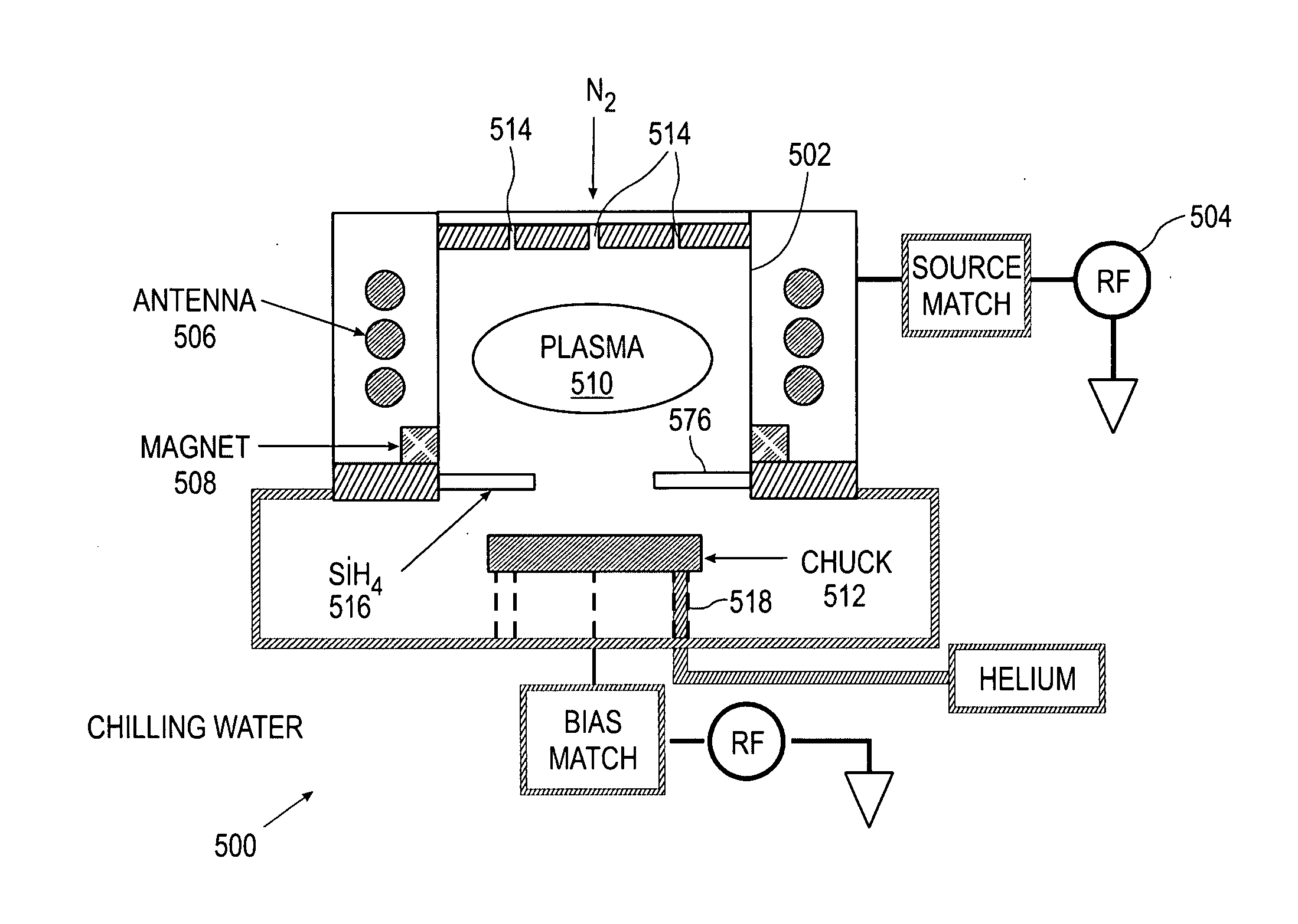
The systems and methods described herein provide for the fabrication of micro-electro-mechanical system (MEMS) components and, as described below, other related system components, on a substrate using a low temperature deposition process. More specifically, the MEMS component can be fabricated on a substrate, such as a printed circuit board (PCB), which would normally be damaged from the high temperatures accompanying typical deposition processes. This is because the deposition process of the present invention takes place at a temperature below the maximum temperature of the substrate. As a result, a MEMS component does not require discrete packaging prior to placement on the substrate. This simplifies the overall fabrication and design processes of a system formed on a low temperature substrate that includes one or more MEMS components and other related system components.

The systems and methods described herein apply to all types of MEMS systems including radio frequency (RF) ME...


PUM


Abstract

Systems and methods are provided that facilitate the formation of micro-mechanical structures and related systems on a laminated substrate. More particularly, a micro-mechanical device and a three-dimensional multiple frequency antenna are provided for in which the micro-mechanical device and antenna, as well as additional components, can be fabricated together concurrently on the same laminated substrate. The fabrication process includes a low temperature deposition process allowing for deposition of an insulator material at a temperature below the maximum operating temperature of the laminated substrate, as well as a planarization process allowing for the molding and planarizing of a polymer layer to be used as a form for a micro-mechanical device.

Description

FIELD OF THE INVENTION The invention relates generally to Micro-Electro-Mechanical Systems (MEMS), and more particularly to the substrate independent fabrication of MEMS structures and related systems on a laminated substrate. BACKGROUND INFORMATION A radio frequency (RF) micro-electro-mechanical system (MEMS) provides lower power, higher performance, wider tuning range, and a freedom of integration which traditional RF components cannot. RF MEMS switches are basic building blocks for a variety of RF circuitry. These switches offer better RF performance, lower insertion loss and more isolation than their semiconductor counterparts such as field effect transistors (FETs) and PIN diodes. In addition, RF MEMS switches can operate at low power levels with a high degree of linearity and very low signal distortion. These features make RF MEMS switches very attractive for RF applications such as radar and communications. Indeed, RF MEMS circuits including variable capacitors, tunable fil...

Claims


Application Information

Patent Timeline
Patent Type & Authority Applications(United States)
IPC IPC(8): H01Q1/38
CPCH01Q1/38
Inventor CETINER, BEDRI A.BACHMAN, MARKLI, GUANN-PYNGQIAN, JIANGYUANCHANG, HUNG-PINDE FLAVIIS, FRANCO
Owner RGT UNIV OF CALIFORNIA
Why Eureka
Try Eureka