Solid state imaging device

a solid-state imaging and imaging device technology, applied in the field of solid-state imaging devices, can solve the problems of imbalanced spectrum sensitivity between the high-sensitive and the low-sensitive photodiodes, difficult that the low-sensitive photodiodes and the high-sensitive photodiodes have the same spectrum sensitivity, and other properties receive a bad influence, so as to prevent a decline in sensitivity

Inactive Publication Date: 2005-03-24
FUJIFILM CORP
View PDF20 Cites 33 Cited by
  • Summary
  • Abstract
  • Description
  • Claims
  • Application Information

AI Technical Summary

Benefits of technology

[0012] It is an object of the present invention to provide a s

Problems solved by technology

Therefore, spectrum sensitivity between the high-sensitive photodiode and the low-sensitive photodiode tends to become imbalanced.
In the solid state imaging device having a structure wherein a fixed colored color filter layer on upper part of each photodiode, it is difficult that the low-sensitive photodiode and the high-sensitive photodiode have same spectrum sensitivity.
Although it is possible to adjus

Method used


Image

  • Solid state imaging device
  • Solid state imaging device
  • Solid state imaging device

Examples


first embodiment

[0040]FIG. 1A, FIG. 1B, FIG. 1C, FIG. 2A, FIG. 2B and FIG. 2C are diagrams for explaining a solid state imaging device according to the present invention.

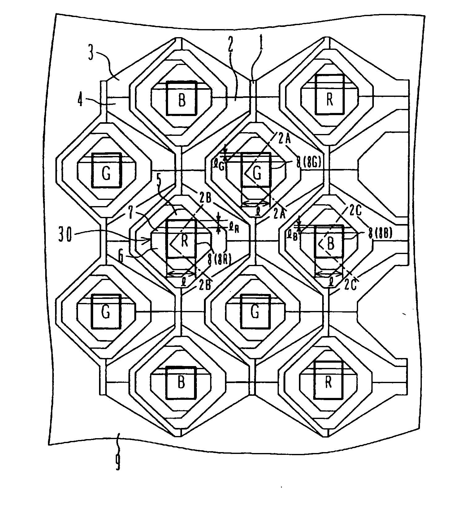
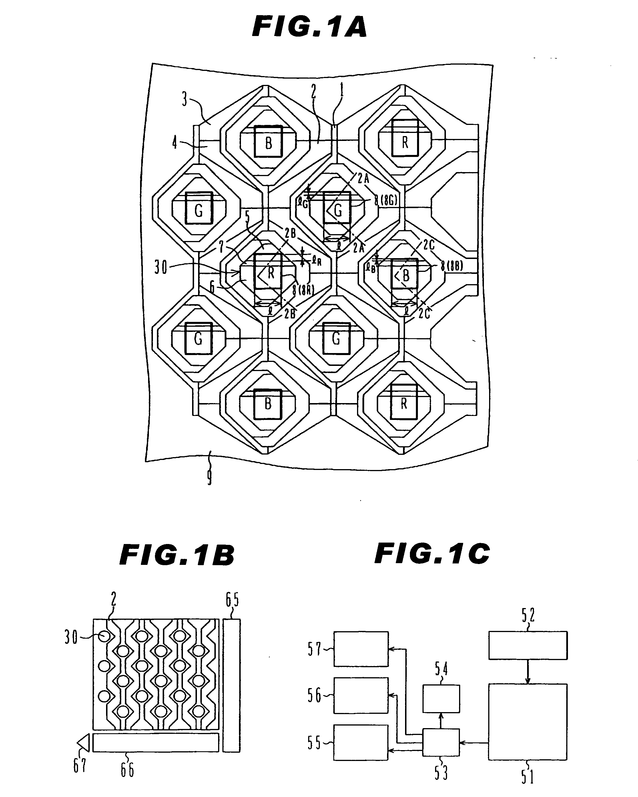
[0041]FIG. 1A is a schematic plan view showing a part of a light receiving region of the solid state imaging device formed on a silicon substrate. Further, in FIG. 1A, in order to avoid complication, some composition elements such as a color filter, a microlens and the like are omitted.

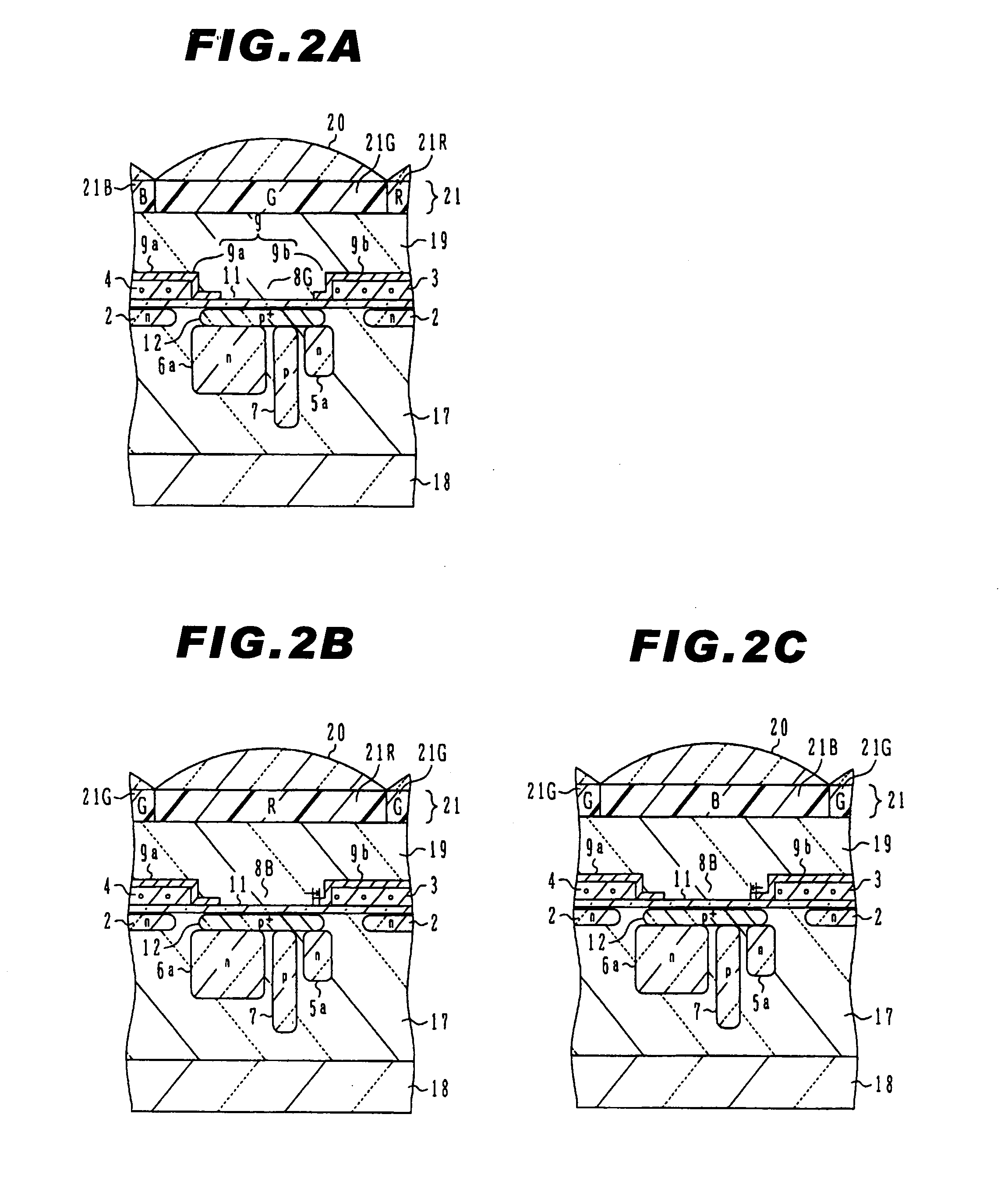
[0042] In FIG. 1A, a plurality of photosensitive regions 30 are shown. Each photosensitive region 30 has electric charge accumulation regions having different area sizes and opening ratios, and it is formed including two photodiodes having different sensitivity, which are the high-sensitive photodiode 6 and the low-sensitive photodiode 5 and a photodiode isolation region 7 provided between the above-described two photodiodes. The high-sensitive photodiode 6 has a relatively large area and consists a main photosensitive part. The low-sensitive photod...

second embodiment

[0100] Next, the present invention will be explained.

[0101] The inventors of the present invention executed a Finite Differential Time Domain Method (FDTD) considering a wave-optical effect, instead of a ray tracing simulation based on the conventional geometric optics, and analyzed a mechanism of sensitivity decline and color shading at a peripheral area of the solid-state imaging device. As a result, it became clear that light concentrating efficiency of each pixel at a peripheral area of the element and miniaturized pixels is depending on the wavelength of the incident light and a phenomenon that sensitivity of a light will be lower as a wavelength of the light (for example, red light (R)) gets longer.

[0102]FIG. 8 is a graph showing a relationship between a pixel (cell) size at a time that an angle of the incident light is fixed and light concentrating efficiency when the incident light achieves a photoelectric conversion element through a micro-lens, a color filter and an openi...

third embodiment

[0137]FIG. 14A is a plan view showing shapes of openings of the light shielding film in the light receiving region of a solid-state imaging device 300 according to the present invention.

[0138] In the third embodiment, opening areas of the openings 108 are varied from the center part CNT to the peripheral part PHL. For example, when the opening area at the center part CNT is L, and the opening area at the peripheral part PHL is L3, the opening area are enlarged from the center part CNT to the peripheral part PHL in order to make L3=({square root}L1) / Sin θ. Moreover, when the opening area of the interval part INT between the center part CNT and the peripheral part PHL in the light receiving region is L2, the openings 108 are formed in order to have a relationship represented by an equation: L123 (or L12≦L3 or L1≦L23).

[0139] By doing that, as shown in FIG. 14B, the effective opening size for the same light source can be maintained to be the same both in the center part CNT and the per...


PUM


Abstract

A solid state imaging device comprises a color decomposer that decomposes incident light into at least a color of a first wavelength and a color of a second wavelength that is shorter than the first wavelength, a light shielding film that is formed under the color decomposer and comprises first openings thorough which light decomposed to the color of the first wavelength and second openings through which light decomposed to the color of the second wavelength, the second openings being formed to be larger than the first openings, and a plurality of photo electric conversion elements that are arranged in lines and columns, each of the photo electric conversion element generating signal electric charge corresponding to an amount of the incident light by receiving the incident light decomposed by the color decomposer and passed through the openings of the light shielding film.

Description

CROSS REFERENCE TO RELATED APPLICATION [0001] This application is based on Japanese Patent Application 2003-327664, filed on Sep. 19, 2003, and Japanese Patent Application 2004-143626, field on May 13, 2004, the entire contents of which are incorporated herein by reference. BACKGROUND OF THE INVENTION [0002] A) Field of the Invention [0003] This invention relates to a solid state imaging device having a plurality of photoelectric conversion elements (photodiodes) in a light receiving region. [0004] B) Description of the Related Art [0005] As a solid state imaging device, a CCD solid state imaging device that transmits a signal charge using a charge coupled device (CCD), a MOS type solid state imaging device that outputs after amplifying a image signal from a photosensitive element with a MOS transistor and the like are well known. The photosensitive elements may be arranged in a tetragonal matrix wherein the elements are arranged in a fixed pitch to a row and a column directions or ...

Claims


Application Information

Patent Timeline
IPC IPC(8): H01L27/14H01L27/146H01L27/148H01L31/0216H04N5/335H04N5/353H04N5/355H04N5/361H04N5/369H04N5/372H04N9/07
CPCH01L27/14621H01L27/14627H01L31/02164H01L27/14818H01L27/14868H01L27/14632
Inventor TAKEUCHI, YUTAKASHIBATA, KATSUHIROUYA, SHINJISHIZUKUISHI, MAKOTO
Owner FUJIFILM CORP
Why Eureka
Try Eureka