Nonvolatile memory cell employing a plurality of dielectric nanoclusters and method of fabricating the same

US20050067651A1Inactive Publication Date: 2005-03-31SAMSUNG ELECTRONICS CO LTD

Image

  • Nonvolatile memory cell employing a plurality of dielectric nanoclusters and method of fabricating the same
  • Nonvolatile memory cell employing a plurality of dielectric nanoclusters and method of fabricating the same
  • Nonvolatile memory cell employing a plurality of dielectric nanoclusters and method of fabricating the same

Examples


Embodiment Construction

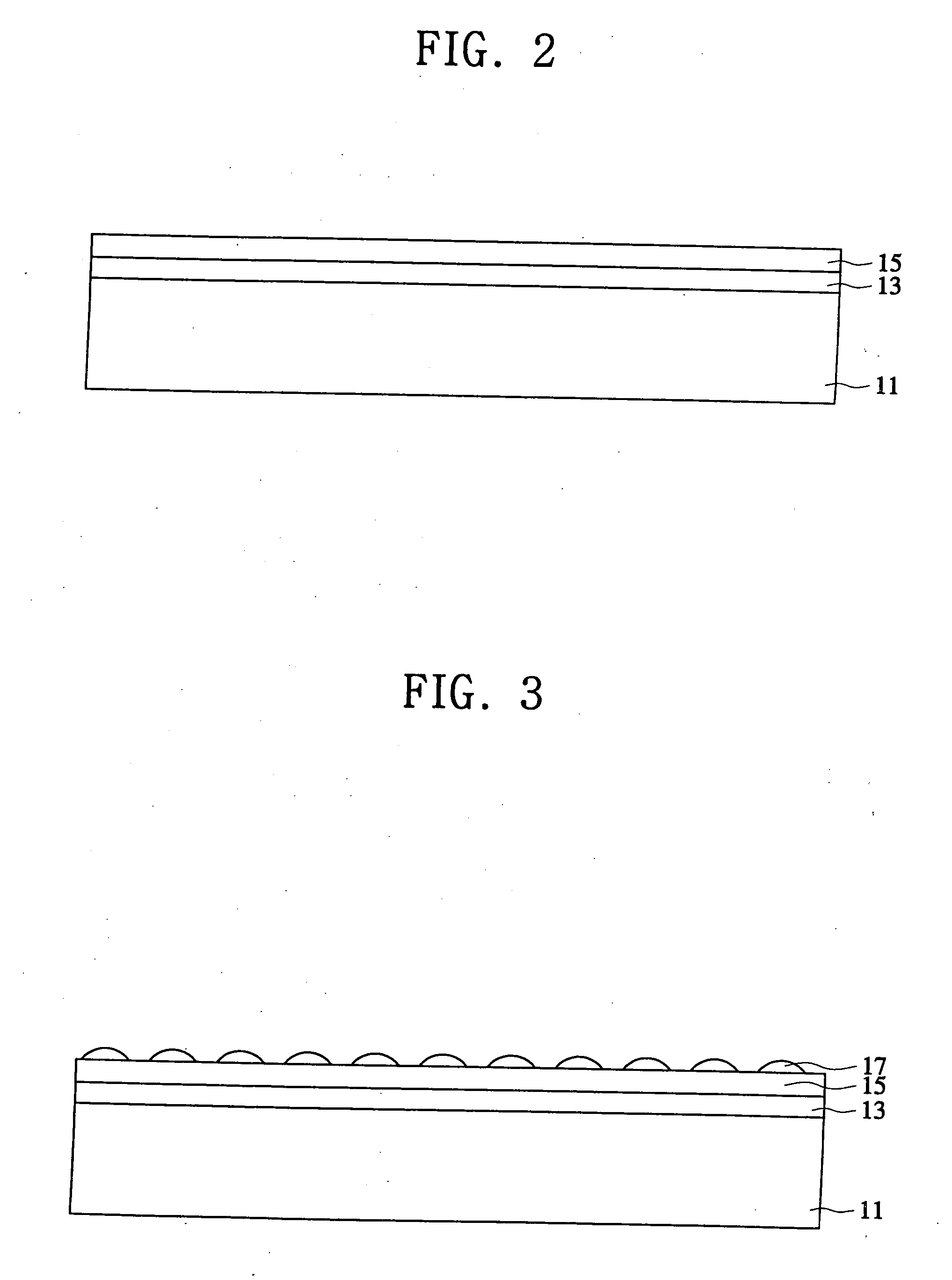
[0033] Embodiments of the present invention will now be described more fully hereinafter with reference to the accompanying drawings, in which preferred embodiments of the invention are shown. The invention may, however, be embodied in different forms and should not be construed as limited to the embodiments set forth herein. Rather, these embodiments are provided so that this disclosure will be thorough and complete, and will fully convey the scope of the invention to those skilled in the art. Like numbers refer to like elements throughout the specification. It will be understood that when an element such as a layer, region or substrate is referred to as being “on” or “onto” another element, it can be directly on the other element or intervening elements may also be present. Additionally, when the layer, region or substrate could be partially within or partially embedded in another element.

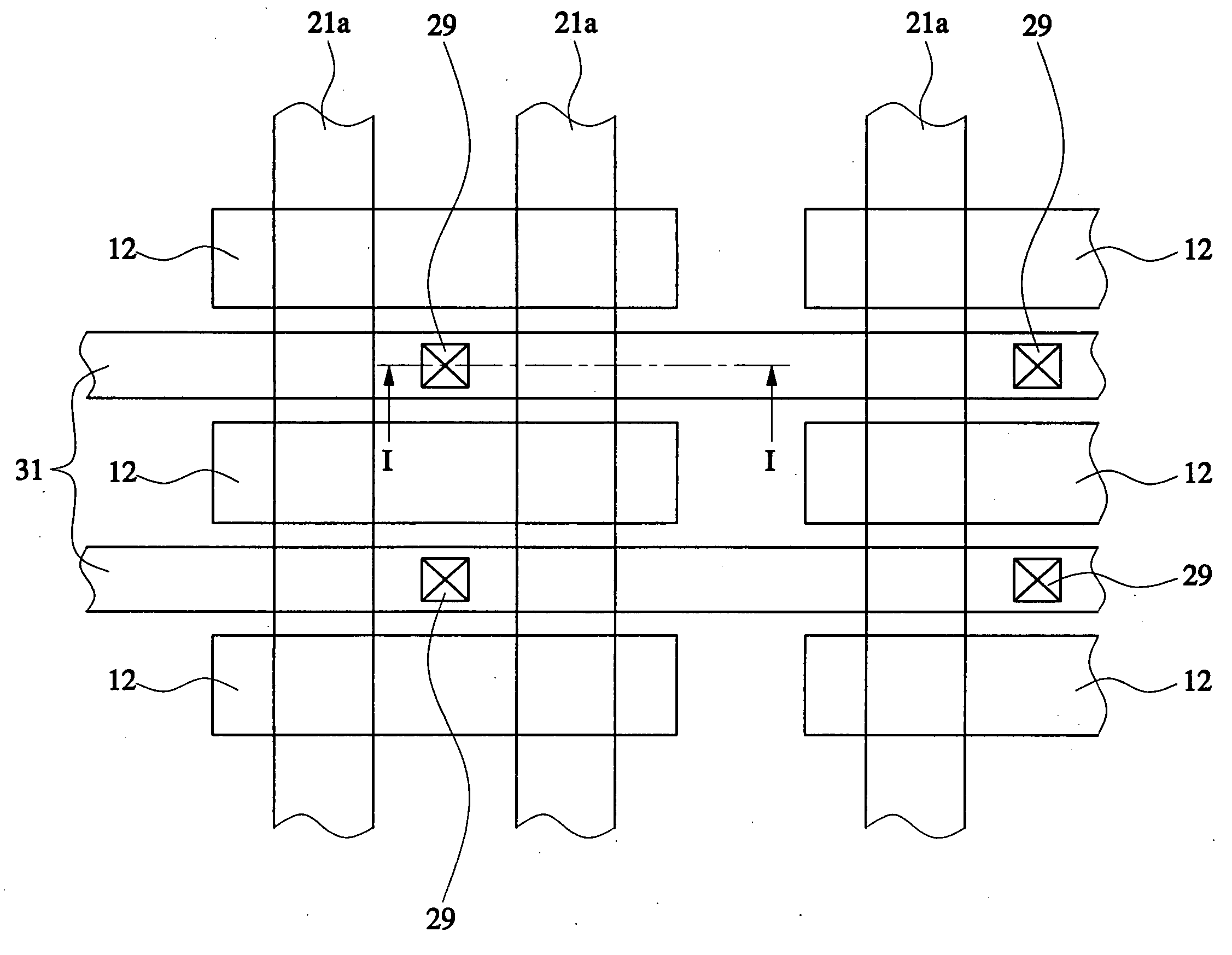
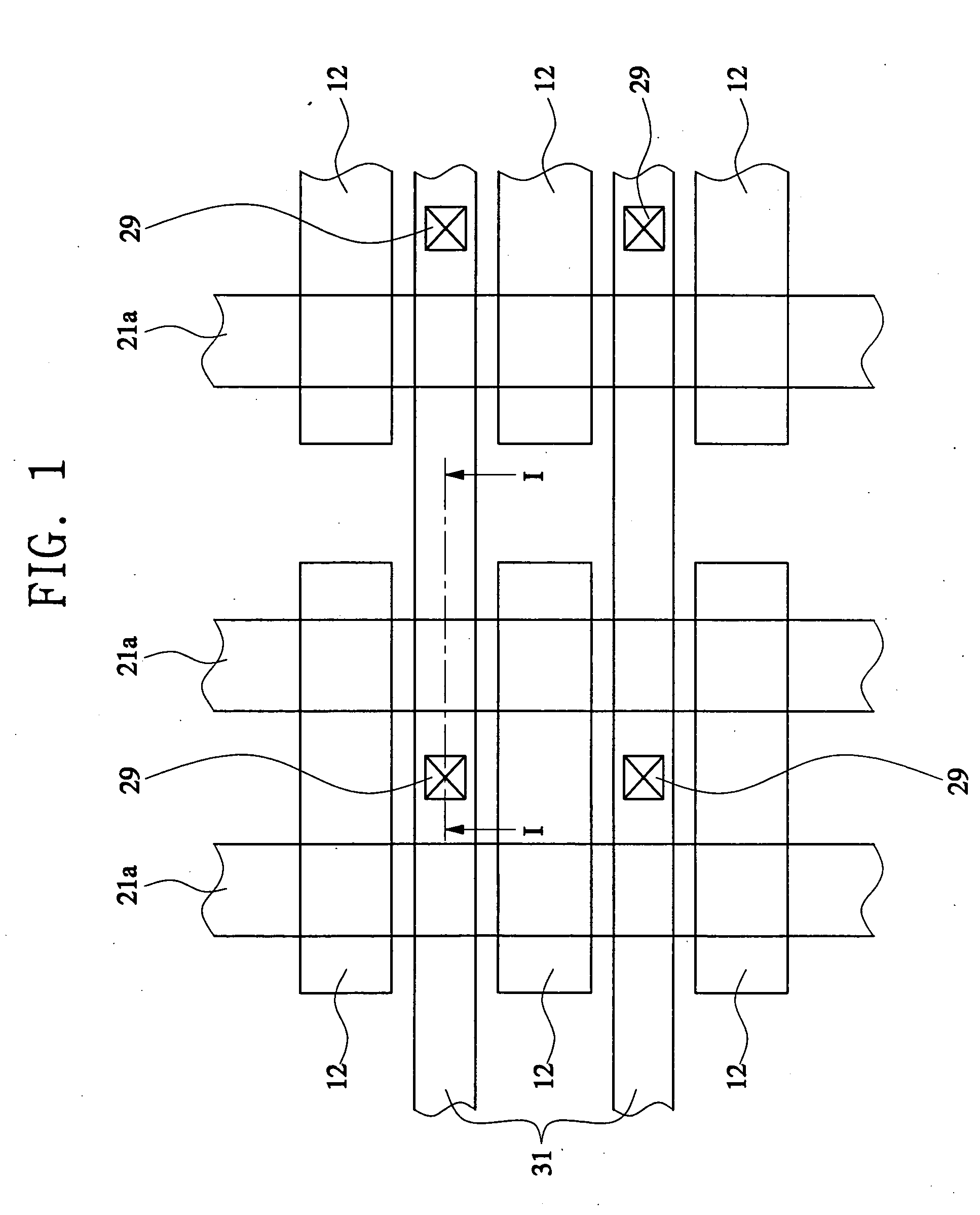
[0034]FIG. 1 is a layout of nonvolatile memory cells according to an embodiment of the prese...


PUM


Abstract

A nonvolatile memory cell employing a plurality of dielectric nanoclusters and a method of fabricating the same are disclosed. In one embodiment, the nonvolatile memory cell comprises a semiconductor substrate having a channel region. A control gate is disposed above the channel region. A control gate dielectric layer is disposed between the channel region and the control gate. A plurality of dielectric nanoclusters are disposed between the channel region and the control gate dielectric layer. Each nanocluster may be separated from adjacent nanoclusters by the control gate dielectric layer. A tunnel oxide layer is disposed between the plurality of dielectric nanoclusters and the channel region. Further, a source and a drain are formed in the semiconductor substrate.

Description

CROSS-REFERENCE TO RELATED APPLICATION [0001] This application claims the benefit of Korean Patent Application No. 2003-66939, filed on Sep. 26, 2003, the disclosure of which is hereby incorporated herein by reference in its entirety. BACKGROUND OF THE INVENTION [0002] 1. Field of the Invention [0003] This disclosure relates to a nonvolatile memory cell and method of fabricating the same and, more particularly, to a nonvolatile memory cell employing a plurality of dielectric nanoclusters and method of fabricating the same. [0004] 2. Description of the Related Art [0005] Nonvolatile memory devices are desired because they retain data even if power is not supplied to them. These devices comprise flash memory and have been widely used in file systems, memory cards, and portable devices, etc. [0006] The nonvolatile memory device may be classified as having a stacked gate structure, a notched gate structure or a nanodot gate structure. The stacked gate structure is characterized in that ...

Claims


Application Information

Patent Timeline
31 Mar 2005
Publication
US20050067651A1
IPC
H01L21/28; H01L27/115; H01L21/336; H01L29/423; H01L29/51; H01L29/792
CPC
B82Y10/00; H01L21/28273; H01L21/28282; H01L29/42332; H01L29/792; H01L29/518; H01L29/66825; H01L29/66833
Inventors
KIM, KI-CHUL; LIM, BYOU-REE