Resist pattern forming method and semiconductor device fabrication method
- Summary
- Abstract
- Description
- Claims
- Application Information
AI Technical Summary
Benefits of technology
Problems solved by technology
Method used
Image

Examples
first embodiment
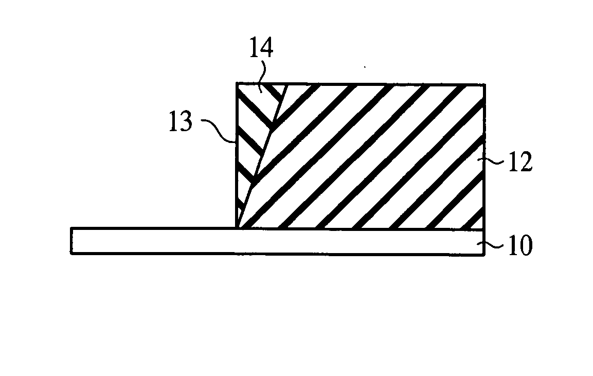
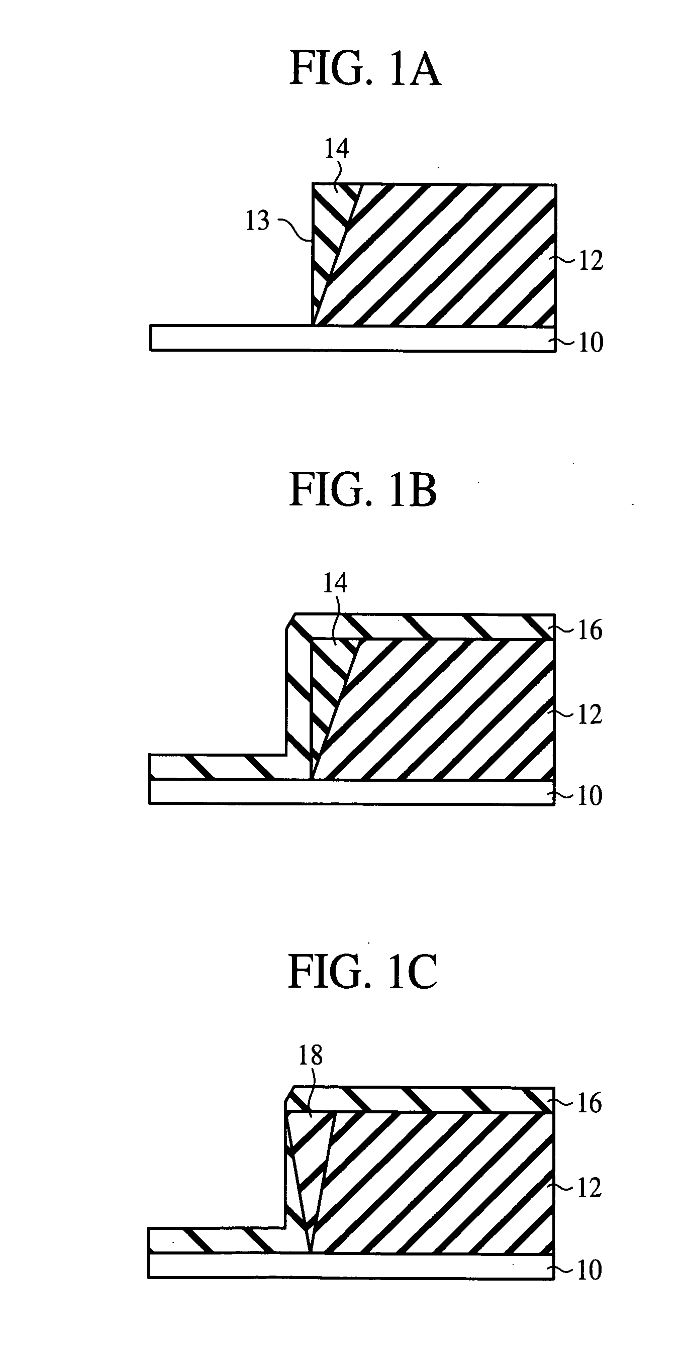
[0036] [A First Embodiment]
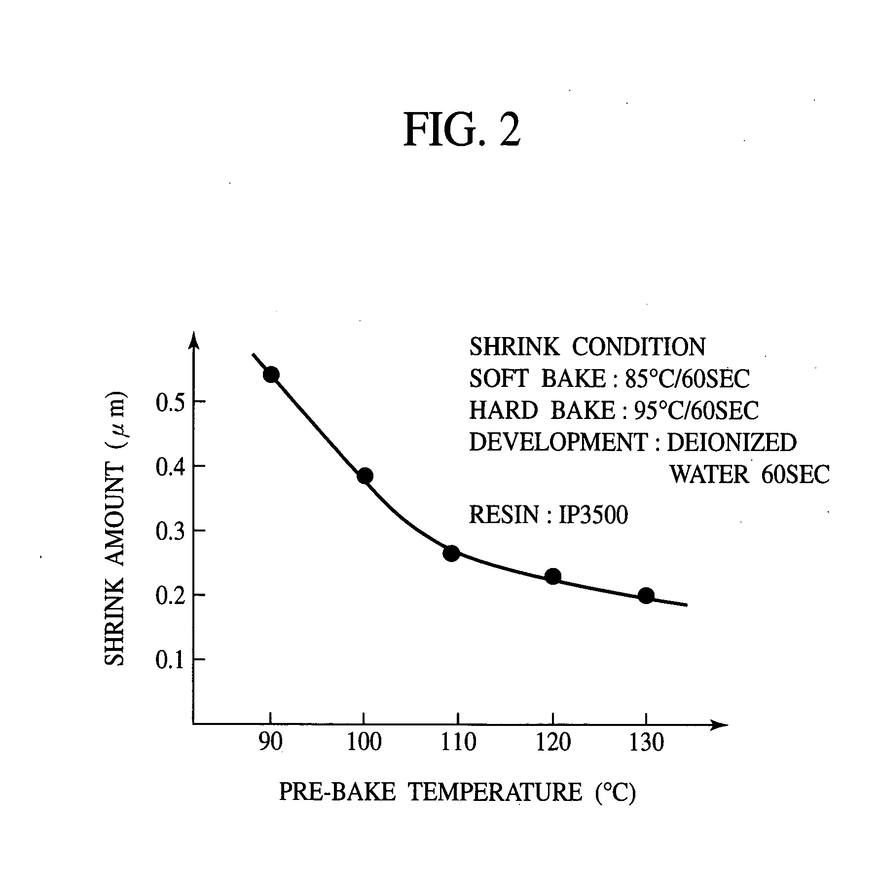
[0037] The resist film forming method according to a first embodiment of the present invention will be explained with reference to FIGS. 1A to 3. FIGS. 1A-1C are sectional views showing the resist pattern forming method according to the present embodiment. FIG. 2 is a graph of relationship between shrinkage amounts and pre-bake temperatures. FIG. 3 is a graph of relationship between shrinkage amounts and kinds of resins.
[0038] As described in, e.g., Reference 4 and Reference 5, as a technique of forming a downsized resist pattern is known a method in which a prescribed auxiliary agent is reacted with a patterned photoresist film to swell the resist pattern to thereby more downsize the pattern formed by the photolithography.
[0039] The inventors of the present application have made earnest studies of the above-described technique and have made it clear for the first time that a patterned novolak-based photoresist is reacted with a prescribed resist pattern...
second embodiment
[0132] [A Second Embodiment]
[0133] The semiconductor device and the method for fabricating the same according to a second embodiment of the present invention will be explained with reference to FIGS. 4 to 6D.
[0134]FIG. 4 is a diagrammatic sectional view of the semiconductor device according to the present embodiment, which shows a structure thereof. FIGS. 5A-5D and 6A-6D are sectional views of the semiconductor device according to the present embodiment in the steps of the method for fabricating the same, which show the method.
[0135] First, the structure of the semiconductor device according to the present embodiment will be explained with reference to FIG. 4.
[0136] An insulating film 22 is formed on a compound semiconductor substrate 20 with a compound semiconductor layer of, InP, GaN or others is formed on. An opening 28 down to the compound semiconductor substrate 20 is formed in the insulating film 22. On the insulating film 22 with the opening 28 formed in, a gate electrode ...
third embodiment
[0155] [A Third Embodiment]
[0156] The semiconductor device and the method for fabricating the same according to a third embodiment of the present invention will be explained with reference to FIGS. 7 to 10C.
[0157]FIG. 7 is a diagrammatic sectional view of the semiconductor device according to the present embodiment, which show a structure thereof. FIGS. 8A-8D, 9A-9C and 10A-10C are sectional views of the semiconductor device according to the present embodiment in the steps of the method for fabricating the same, which show the method.
[0158] First, the structure of the semiconductor device according to the present embodiment will be explained with reference to FIG. 7.
[0159] A buffer layer 42 of InAlAs is formed on an InP substrate 40. On the buffer layer 42, a channel layer 44 of InGaAs is formed. A carrier-supplying layer 46 of InAlAs is formed on the channel layer 44. The carrier-supplying layer 46 has the layer structure of i-InAlAs / n-InAlAs / 1-InAlAs. On the carrier-supplying l...
PUM
 Abstract
Description
Claims
Application Information
 - Generate Ideas
- Intellectual Property
- Life Sciences
- Materials
- Tech Scout
- Unparalleled Data Quality
- Higher Quality Content
- 60% Fewer Hallucinations
Browse by: Latest US Patents, China's latest patents, Technical Efficacy Thesaurus, Application Domain, Technology Topic, Popular Technical Reports.
© 2025 PatSnap. All rights reserved.Legal|Privacy policy|Modern Slavery Act Transparency Statement|Sitemap|About US| Contact US: help@patsnap.com