Etching method and computer storage medium storing program for controlling same

a technology of computer storage medium and etching method, which is applied in the direction of microlithography exposure apparatus, electrical apparatus, photosensitive material processing, etc., can solve the problems of preventing the formation of desired pattern forms, uneven pattern widths in the patterned mask layer, and affecting the fineness of the circuit, so as to reduce the pattern width of the mask layer increase the pattern width

Active Publication Date: 2005-03-31
TOKYO ELECTRON LTD
View PDF7 Cites 37 Cited by
  • Summary
  • Abstract
  • Description
  • Claims
  • Application Information

AI Technical Summary

Benefits of technology

[0015] In accordance the present invention, there are provided an etching method and a computer readable storage medium storing therein a program for controlling same, the etching method including the steps of: a first process for increasing pattern widths of a pre-patterned mask layer by depositing plasma reaction products on sidewalls of the mask layer; and a second process for etching a layer to be etched by using the mask layer as a mask having the increased pattern widths. According to this method, even though the pattern width of a previously patterned mask layer deviates from a design value, the deviation can be corrected. Further, it is preferable that the second process is performed by etching the layer to be etched while reducing the pattern widths of the mask layer by etching the sidewalls thereof. In the second process, the pattern widths of the mask layer are reduced, it is possible to adjust the pattern widths to a fine value. Still further, a processing gas of the first process includes at least any one of a CF based gas, a CHF based gas and a CH based gas. For example, when CHF3 is used as a processing gas, the pattern widths of the mask layer are efficiently increased in the first process.
[0016] In accordance with the present invention, there are provided an etching method and a computer readable storage medium storing therein a program for controlling same, the etching method including the steps of: a first process for etching sidewalls of a pre-patterned mask layer to produce a processed mask layer with reduced pattern widths; and a second process for

Problems solved by technology

In a conventional exposure processing, if a light irradiated onto a photoresist film is diffusely reflected on an interface between the photoresist film and an under film, the light reaches regions of the photoresist film where it is not supposed to, thus possibly preventing a desired pattern form being obtained.
In light of a current trend toward the fineness of circuit patterns and, particularly, its corresponding change of a light source from a KrF excimer laser (248 nm) to a short wave ArF excimer laser (193 nm), this phenomenon has been a problem.
The unevenness in the sidewall shapes of the BARC is hindrance to the fineness of the circu

Method used


Image

  • Etching method and computer storage medium storing program for controlling same
  • Etching method and computer storage medium storing program for controlling same
  • Etching method and computer storage medium storing program for controlling same

Examples


first embodiment

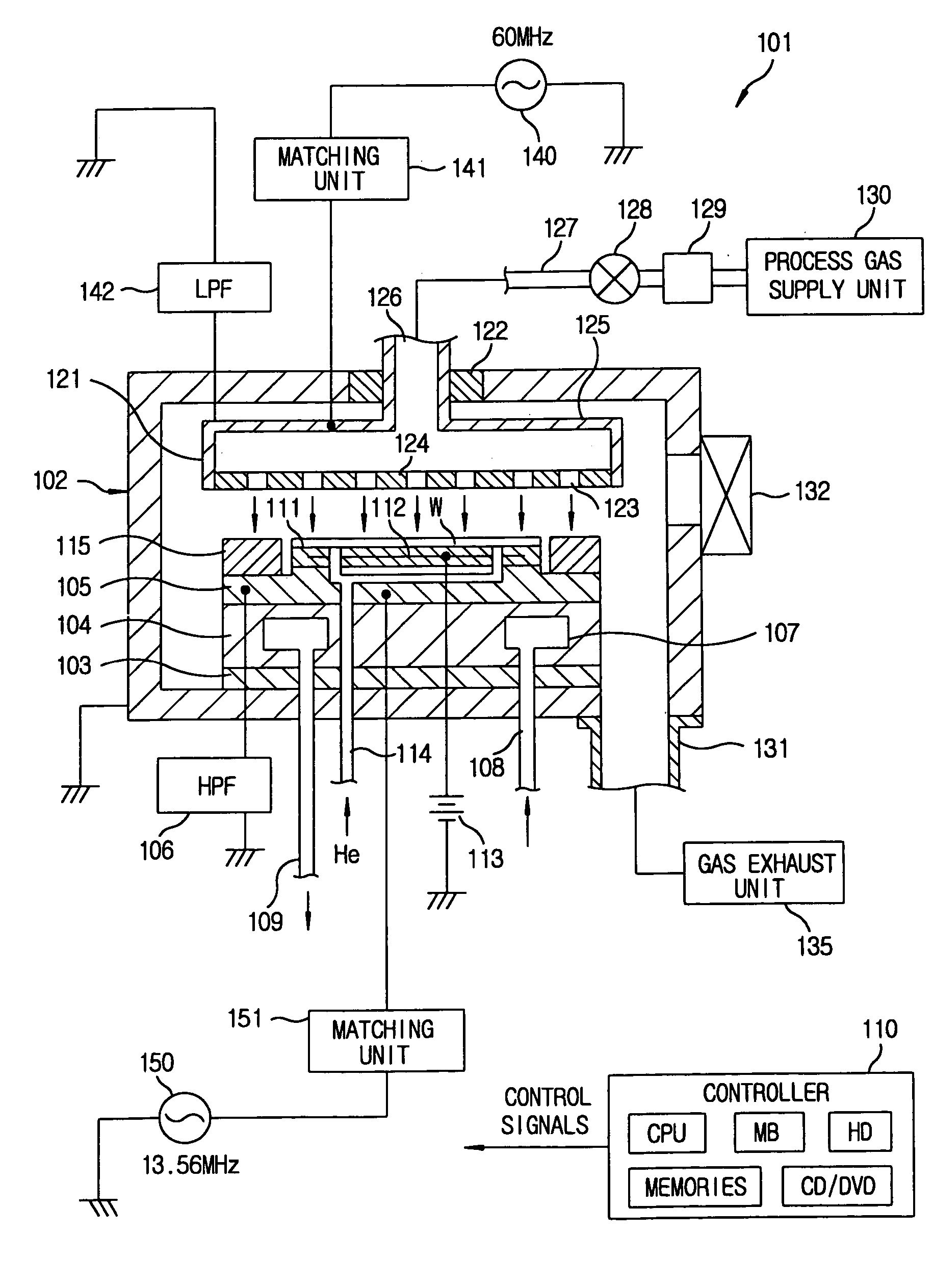
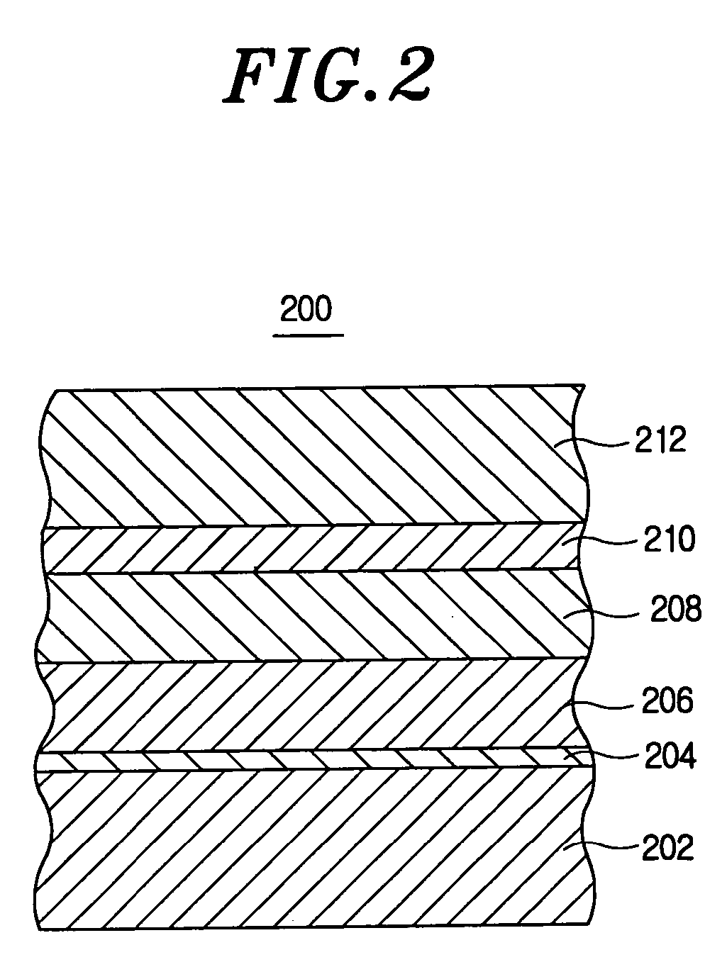
[0060] In accordance with the present invention, even in case where the deviation exists in the pattern widths of the mask layer 212 patterned by using the photolithography technology, it is possible to eliminate the deviation and form an even circuit over the entire wafer. Hereinafter, an etching method in accordance with the present invention will be explained.

[0061] (First Embodiment)

[0062] In the present embodiment, a mask layer 212 is used as a mask, and a plasma etching process is performed selectively on a BARC (a layer to be etched) 210 disposed below the mask layer 212. The plasma etching process is performed in at least two processes (first and second processes) having different process conditions.

[0063] First, reaction products are deposited on sidewalls of a pre-patterned mask layer 212 prepared by using a photolithography process, and process conditions are set to increase each pattern width. Further, the process conditions are set to allow a pattern width L110 of a m...

second embodiment

[0098] (Second Embodiment)

[0099] Next, a second embodiment of the present invention will be described with reference to the attached drawings. In the example of the first embodiment shown in FIG. 3A, the pattern width L120 of the mask layer 212-2 pertaining to the second region regl2 (low pattern density region) was narrower than the pattern width L110 of the mask layer 212-1 pertaining to the first region reg11 (high pattern density region). However, when the photolithography process is performed on the mask layer 212 and the mask layer 212 is patterned, the opposite phenomenon may occur. Namely, as shown in FIG. 8A, a pattern width L220 of a mask layer 212-2 pertaining to a second region reg22 (low pattern density region) may be wider than a pattern width L210 of a mask layer 212-1 pertaining to a first region reg21 (high pattern density region).

[0100] Accordingly, the second embodiment describes an example, in which, even though a difference shown in FIG. 8A exists in pattern wi...


PUM


Abstract

An etching method of the present invention includes a first and a second process. In the first process, pattern widths of a pre-patterned mask layer are increased by depositing plasma reaction products on sidewalls of the mask layer. In the second process, a layer to be etched is etched by using the mask layer as a mask having increased the pattern widths. Therefore, mask layers having different pattern densities exist in the same wafer and pattern widths of mask layers patterned through a photolithography process are uneven according to pattern densities, each pattern width of the mask layers can be made uniform. Accordingly, the pattern widths of the layer can be made uniform over an entire wafer.

Description

FIELD OF THE INVENTION [0001] The present invention relates to an etching method and a computer readable storage medium storing therein a program for controlling same. BACKGROUND OF THE INVENTION [0002] In order to manufacture a semiconductor device, an etching process of forming desired fine patterns on a film formed on a semiconductor wafer (hereinafter referred to as a “wafer”) is performed. In the etching process, a photolithography technology is employed to form fine pattern circuits. Specifically, a photoresist material is uniformly coated to a layer to be etched and dried, first. Thereafter, in an exposing step, a photoresist film is exposed to a light having a predetermined wavelength, and the fine pattern circuits are transferred thereto. [0003] For example, in case where the photoresist material is of a positive type, the portions of the photoresist film, onto which the light has been irradiated, are removed by developing, thus forming a patterned mask layer. Subsequently,...

Claims


Application Information

Patent Timeline
IPC IPC(8): H01L21/3065G03F7/20H01L21/00H01L21/02H01L21/027H01L21/033H01L21/311H01L21/3213
CPCH01L21/0337H01L21/32139H01L21/31138G03F7/40
Inventor KUSHIBIKI, MASATOSAWATAISHI, MASAYUKISHIMIZU, AKITAKA
Owner TOKYO ELECTRON LTD
Why Eureka
Try Eureka