Socket and contact of semiconductor package

a semiconductor and socket technology, applied in the direction of fixed connections, electrical apparatus construction details, coupling device connections, etc., can solve the problems of reducing the inability to perform high-precision testing or evaluation of the semiconductor package in a high frequency range, and the need for further reduction of the height of the socket, so as to facilitate manufacturing

Inactive Publication Date: 2005-03-31
MOLEX INC
View PDF1 Cites 2 Cited by
  • Summary
  • Abstract
  • Description
  • Claims
  • Application Information

AI Technical Summary

Benefits of technology

[0027] It is preferable that a pull-off preventing projection for preventing pull-off from the socket body is provided in the support piece. With the pull-off preventing projection, i

Problems solved by technology

This causes a problem that the test or evaluation of the semiconductor package could not be performed with high precision in a high frequency range.
The same problem arises also in the case of a socket comprising a contact in which, as shown in FIG. 16, contact portions are formed at its respective upper and lower ends, and a spring is provided between the contact portions.
However, also in this technique, there are problems to be solved as described below.
Namely, these are problems associated with th

Method used


Image

  • Socket and contact of semiconductor package
  • Socket and contact of semiconductor package
  • Socket and contact of semiconductor package

Examples


Embodiment Construction

[0045] While the invention may be susceptible to embodiment in different forms, there is shown in the drawings, and herein will be described in detail, a specific embodiment with the understanding that the present disclosure is to be considered an exemplification of the principles of the invention, and is not intended to limit the invention to that as illustrated and described herein.

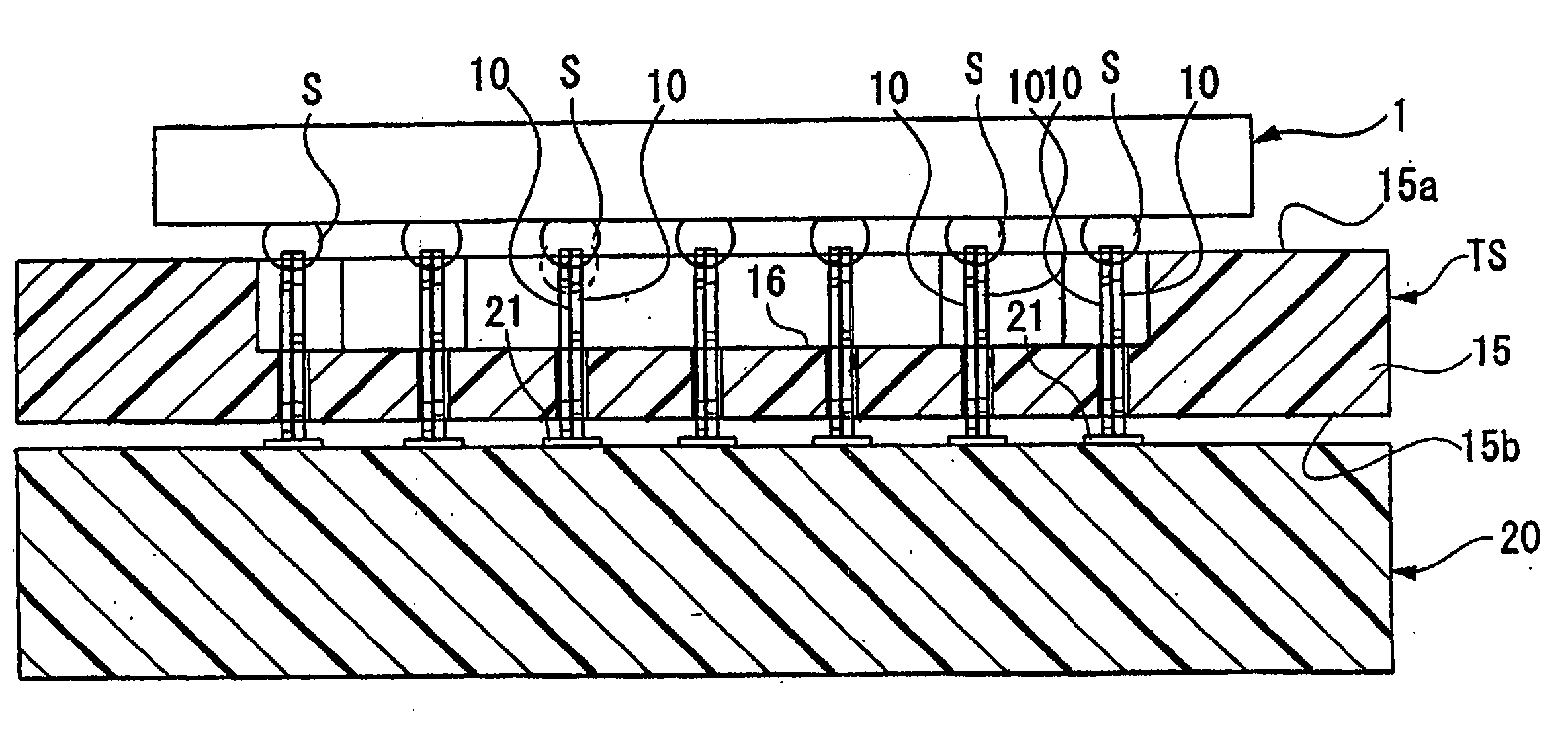
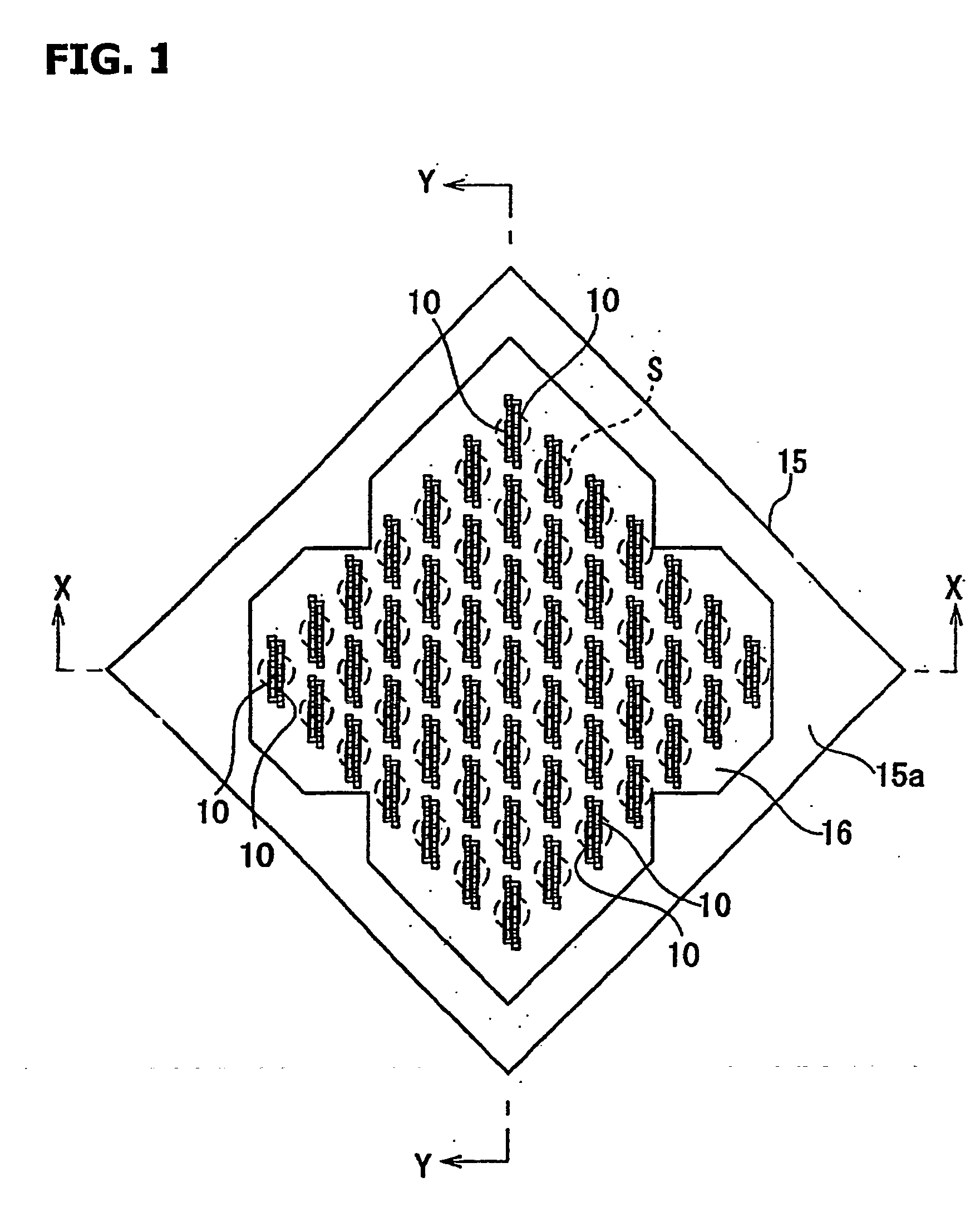
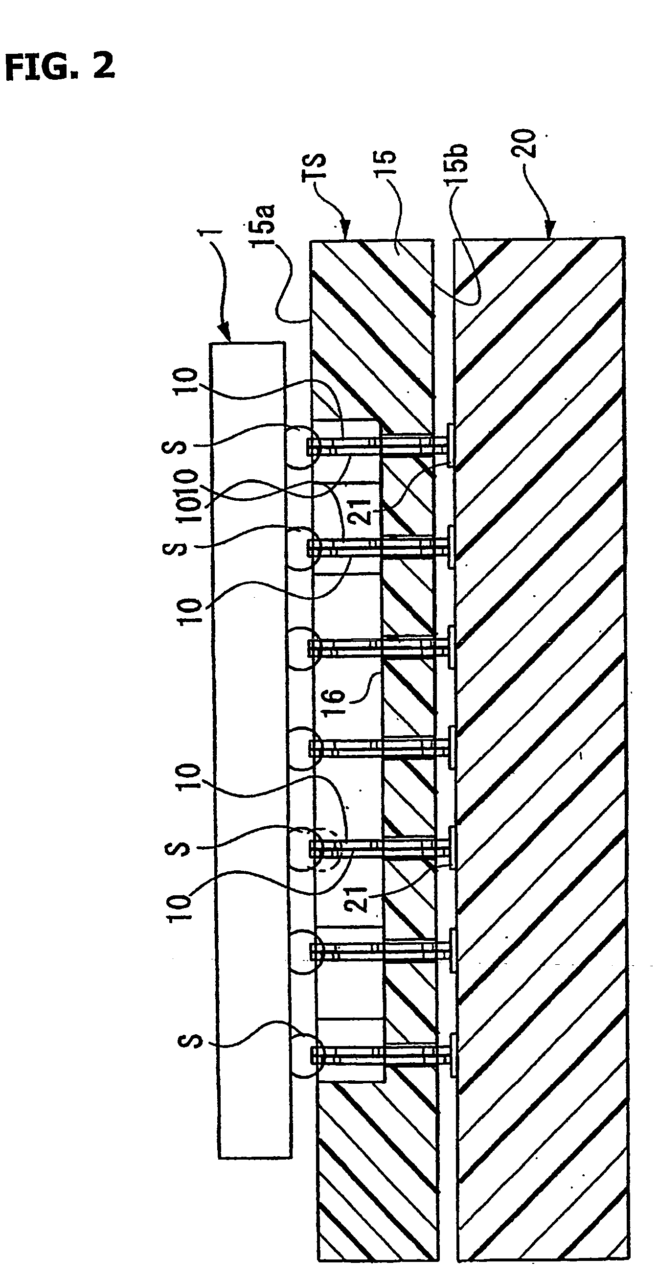
[0046]FIG. 1 is a plan view of a socket (test socket) of a semiconductor package in accordance with the embodiment of the present invention. FIG. 2 is a cross-sectional view taken along the line X-X of FIG. 1. FIG. 3 is a cross-sectional view taken along the line Y-Y of FIG. 1. FIG. 4 is a partially enlarged view of FIG. 3. FIG. 5 is a view illustrating a contact, and FIG. 6 is a plan view of the socket.

[0047] The test socket TS shown in these drawings is a BGA (Ball Grid Array) testing and evaluating socket of a semiconductor package 1 having a plurality of solder balls S arranged in an array on its ...


PUM


Abstract

The present invention is directed to a socket connector having a plurality of contacts for contacting with a plurality of solder balls arranged on one of the surface of a semiconductor package, and a socket body in which a plurality of mounting holes are provided for mounting respective contacts. The mounting hole is provided with a through-hole pierced in a height direction of the socket body and a contact support hole of the contact. Each contact is provided with an upright piece extending through the through-hole, and a support piece extending from the upright piece to be inserted into the support hole. A contact portion for contacting with the solder ball is formed at a tip end portion of the upright piece. The support piece extends from the proximal end portion of the upright piece.

Description

FIELD OF THE INVENTION [0001] The present invention relates to a socket of a semiconductor package provided with a plurality of contacts for contacting with a plurality of solder balls arranged in an array on one side of the semiconductor package, and such contacts. BACKGROUND OF THE INVENTION [0002] Recently, the reduction of a pitch of integrated circuits has been advancing due to the demand of miniaturization of information processing equipment and high-speed performance thereof. In accordance with this, the actual mounting system is changing from a through-hole type to a surface mounting type and the arrangement of terminals is changing from a peripheral arrangement to an array arrangement. Furthermore, of such array arrangements, a ball grid array (BGA) in which solder balls are arranged in an array-like arrangement on a surface of a package is becoming a main type of a package on which the terminals may be mounted on the surface. [0003] In the case where a socket is used betwe...

Claims


Application Information

Patent Timeline
IPC IPC(8): H01R13/24H01R43/02H05K7/10
CPCH01R9/096H05K7/1069H01R43/0249H01R13/2485H01R12/52
Inventor ADACHI, KIYOSHIYAGI, MASANORI
Owner MOLEX INC
Why Eureka
Try Eureka