Supercharge Your Innovation With Domain-Expert AI Agents!

Grounded-emitter circuit, and high-frequency receiver and high-frequency transmitter using the same

a technology of grounded emitter and receiver, which is applied in the direction of amplifiers, electrical devices, and semiconductor devices/discharge tubes, etc., can solve the problems of preventing sufficient canceling, generating errors in output level and phase, and unable to integrate such an image removing filter into a semiconductor ic. achieve the effect of increasing output level

Inactive Publication Date: 2005-03-31
SHARP KK
View PDF8 Cites 0 Cited by
  • Summary
  • Abstract
  • Description
  • Claims
  • Application Information

AI Technical Summary

Benefits of technology

[0014] With this, it is possible to provide a grounded-emitter circuit capable of being built in an IC, and, in a simple circuit configuration, capable of removing an image frequency signal.
[0018] With these arrangements, in addition to the second impedance circuit whose impedance is a parallel resonance circuit consisting of an inductor and a capacitor, the load impedance circuit provided between the reference voltage and the collector of the transistor is composed of a parallel resonance circuit consisting of an inductor and a capacitor. As described earlier, the impedance of an LC parallel resonance circuit is extremely large with respect to a frequency in the vicinity of the resonance frequency. This enables the grounded-emitter circuit to increase the load impedance and the transfer conductance with respect to a certain frequency. Since the resonance frequency of the first impedance circuit is set differently from the resonance frequency of the second impedance circuit, it is possible to attenuate a certain frequency component and amplify another frequency component at the same time.
[0021] With these arrangements, a grounded-emitter circuit that can attenuate a certain frequency component is provided at a preceding stage of the frequency converter. Therefore it is possible to remove an image frequency component which causes a problem in the frequency converter. This can eliminate the need for an image removing filter and an image removing frequency converter. Further, since the resonance frequency of the parallel resonance circuit of the first impedance circuit is set in the vicinity of the desired signal frequency of the receiver, it is possible to increase a level difference between the desired frequency component and the image frequency component.
[0027] With these arrangements, in a case where the signal generating section of the high-frequency receiver outputs a signal whose frequency is equal to the image frequency of the frequency converter, the grounded-emitter circuit attenuates this signal. If a current component of the image frequency contained in the output signal from the grounded-emitter circuit is large, a radiation field due to the current is also large. Hence the radiation field of the output signal is detected by the field intensity detecting section. If the output level is higher than a desired level, the control section changes the capacitance value of the variable capacitor, so as to attenuate the output level. With this, it is possible to adjust the resonance frequency of the LC parallel resonance circuit so as to achieve desired characteristics, even if the resonance frequency varies due to process variation, a parasitic component, and the like.
[0028] On the other hand, in a case where the signal generating section of the high-frequency receiver outputs a signal whose frequency is equal to the desired frequency, it is possible to achieve similar effects by adjusting the variable capacitor so as to increase the output level.
[0031] With these arrangements, a grounded-emitter circuit that can attenuate a certain frequency component is provided at a subsequent stage of the frequency converter. Therefore it is possible to remove a side band frequency component which causes a problem in the frequency converter. This can eliminate the need for an image removing filter and an image removing frequency converter. Further, if the resonance frequency of the parallel resonance circuit of the first impedance circuit is set in the vicinity of the desired output signal frequency of the transmitter, it is possible to increase a level difference between the desired frequency component and the side band signal component.

Problems solved by technology

A significant problem in the heterodyne system is an image signal.
However, it is difficult to integrate such an image removing filter into a semiconductor IC.
If built in a semiconductor IC, however, the 90-degree phase shifter generates errors in output level and phase, due to process variation, a parasitic component, and the like, and these errors prevent sufficient canceling of the image signal.
However, the bandpass filter and image removing frequency converter prevent reduction of the size and cost of the high-frequency transmitter, or lower the yield of ICs, as explained earlier.
However, the image removing filter is difficult to be integrated into an IC, thus becoming a problem in reducing the size and cost of the transmitter and receiver.
This complicates the circuit, and increases the power consumption of the transmitter and receiver.
Moreover, the 90-degree phase shifter generates a level error and phase error due to process variation, thus causing such a problem that the yield of ICs is lowered.

Method used


Image

  • Grounded-emitter circuit, and high-frequency receiver and high-frequency transmitter using the same
  • Grounded-emitter circuit, and high-frequency receiver and high-frequency transmitter using the same
  • Grounded-emitter circuit, and high-frequency receiver and high-frequency transmitter using the same

Examples


Embodiment Construction

[0054] With reference to FIGS. 1 through 11, the following will explain an embodiment of the present invention.

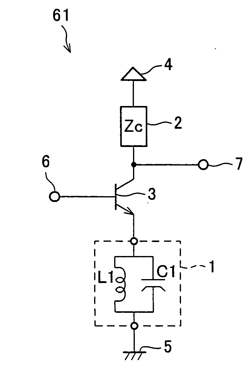
[0055] First, FIG. 11 shows a grounded-emitter circuit 51 which is a basic model of a grounded-emitter circuit in accordance with the present embodiment. The grounded-emitter circuit 51 is a grounded-emitter amplification circuit in which the emitter of a transistor is grounded to GND via an impedance. The grounded-emitter circuit 51 is provided with a transistor 3, a first impedance circuit 2, and a second impedance circuit 1. The transistor 3 is an NPN transistor, and the base of the transistor 3 is an input terminal 6 of the grounded-emitter circuit 51. The emitter of the transistor 3 is grounded to GND 5 via the second impedance circuit 1. The collector of the transistor 3 is connected to a reference voltage source 4 via the first impedance circuit 1, and is an output terminal 7 of the grounded-emitter circuit 51.

[0056] In the grounded-emitter circuit 51 as described ...


PUM


Abstract

A grounded-emitter circuit is composed of a transistor, a first impedance circuit, and a second impedance circuit. The transistor is an NPN transistor, and the base of the transistor is an input terminal of the grounded-emitter circuit. The emitter of the transistor is grounded to GND via the second impedance circuit. The collector of the transistor is connected to a reference voltage source via the first impedance circuit, and is an output terminal of the grounded-emitter circuit. Further, the second impedance circuit is composed of a parallel resonance circuit consisting of an inductor and a capacitor. With this, it is possible to provide a grounded-emitter circuit capable of being built in an IC, and capable of removing an image frequency signal in a simple circuit configuration.

Description

[0001] This Nonprovisional application claims priority under 35 U.S.C. § 119(a) on Patent Application No. 337662 / 2003 filed in Japan on Sep. 29, 2003, the entire contents of which are hereby incorporated by reference. FIELD OF THE INVENTION [0002] The present invention relates to a grounded-emitter circuit; and a transmitter and receiver used in a high frequency band of a wireless communications system, etc. BACKGROUND OF THE INVENTION [0003] As an architecture for a receiver of a wireless communications system, a heterodyne system is widely known. The system is to convert an RF reception signal into a low-frequency signal (IF signal) using a frequency converter (mixer). An example of the arrangement and operation of a heterodyne receiver will be explained with reference to FIG. 12. The RF reception signal is amplified by an LNA circuit 8, and an image frequency component of the RF reception signal is removed by an image removing filter 9. Then, by a frequency converter 10, the sign...

Claims


Application Information

Patent Timeline
Patent Type & Authority Applications(United States)
IPC IPC(8): H04B1/04H04B1/26H03F3/195H04B1/28
CPCH04B1/28
Inventor SAKURAI, SHOJI
Owner SHARP KK
Features
  • R&D
  • Intellectual Property
  • Life Sciences
  • Materials
  • Tech Scout
  • Unparalleled Data Quality
  • Higher Quality Content
  • 60% Fewer Hallucinations
Learn More