Light emitting device

a light-emitting device and light-emitting technology, which is applied in the direction of semiconductor laser arrangement, semiconductor laser structure details, semiconductor lasers, etc., can solve the problems of difficult design for downsizing the laser scanning unit, difficult to drive the semiconductor laser under a suitable matching condition, and ringing or overshooting, so as to improve the output performance of light and reduce the size

Inactive Publication Date: 2005-04-07
ASAHI KOGAKU KOGYO KK
View PDF12 Cites 26 Cited by
  • Summary
  • Abstract
  • Description
  • Claims
  • Application Information

AI Technical Summary

Benefits of technology

[0010] The present invention is advantageous in that it provides a light emitting device which is configured to improve output performance of light and to reduce its size.

Problems solved by technology

However, such an arrangement may raise a problem that a ringing or overshoot arises on a driving signal for the laser diode chip because of a relatively long length of wirings between the laser diode and the control circuit board.
For this reason, it may become difficult to drive the semiconductor laser under a suitable matching condition because of parasitic capacitance and resistance of the connection pattern between the laser diode chip in the package of the semiconductor laser and the driving circuit on the controller board.
In addition to the disadvantage indicated above, use of the configuration disclosed in the publication may cause a problem that the design for downsizing the laser scanning unit becomes difficult because the controller board is supported together with the optical system in the laser scanning unit.

Method used


Image

  • Light emitting device
  • Light emitting device
  • Light emitting device

Examples


first embodiment

[0043] First Embodiment

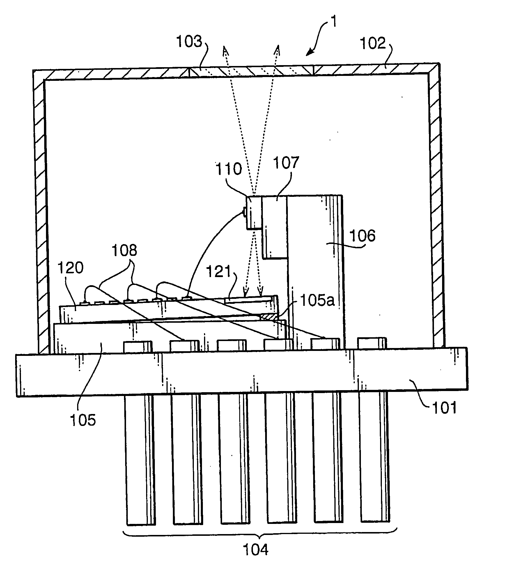
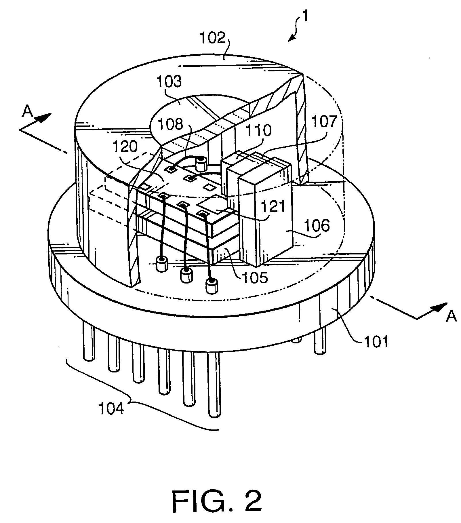
[0044] Hereafter, a laser diode according to a first embodiment of the invention will be described. FIG. 2 is a perspective view of the laser diode 1 according to the first embodiment of the invention. For illustration purpose of an internal configuration, a cap 102 is opened partially. FIG. 3 is an enlarged cross sectional view of the laser diode 1 along a line A-A in FIG. 2. As shown in FIGS. 2 and 3, the laser diode 1 is configured such that a laser diode chip 110 and a driver chip 120 are integrally mounted in a package.

[0045] Specifically, the laser diode 1 includes a circular stem 101 on which a mount 105 and a post 106 are fixed. On the stem 101, a cylindrical cap 102 is fixed to cover and protect internal components. By the stem 101 and the cap 102, the package is configured.

[0046] On the mount 105, the driver chip 120 is mounted. The laser diode chip 110 is attached to a tip portion of the post 106 via a heatsink 107. On the top surface of the packa...

second embodiment

[0060] Second Embodiment

[0061] A laser diode 1A according to a second embodiment will be described. The laser diode 1A is configured as a variation of the laser diode 1 according to the first embodiment. Since an outward appearance of the laser diode 1A is the same as that of the laser diode 1, only a cross sectional view of the laser diode 1A (FIG. 5) is shown to describe the configuration of the laser diode 1A. FIG. 5 corresponds to the cross sectional view of FIG. 3 along the line A-A in FIG. 2. In FIG. 5, to elements, which are the same as those of the first embodiment, same reference numbers are assigned, and explanations thereof will not be repeated.

[0062] As shown in FIG. 5, in this embodiment, a photodiode chip 130 is mounted on the mount 105 as a discrete member. The photodiode chip 130 is connected to a driver chip 120A, which is also mounted on the mount 105, via bonding wires. The driver chip 120A includes the elements indicated in FIG. 4 excepting the photodiode 121.

[...

fourth embodiment

[0078] Fourth Embodiment

[0079]FIG. 8 is a cross sectional view of a laser diode 1C according to a fourth embodiment. The laser diode 1C is configured as a variation of the laser diode 1B of the third embodiment. That is, the laser diode 1C is a surface-mount device.

[0080] Since an outward appearance of the laser diode 1C is substantially the same as that of the laser diode 1B, only a cross sectional view of the laser diode 1C (FIG. 8) is shown to describe the configuration of the laser diode 1C. The cross sectional view of FIG. 8 corresponds to the cross sectional view of FIG. 7 along the line B-B in FIG. 6. In FIG. 8, to elements, which are the same as those of the above mentioned embodiments, same reference numbers are assigned, and explanations thereof will not be repeated.

[0081] As shown in FIG. 8, on the base 141, which is a lead frame having the leads 142, a thermal insulation plate 145 is mounted. A mount 146 and a mount 147 respectively functioning as heatsinks are mounted...


PUM


Abstract

There is provided a light emitting device, which is provided with a light emitting element that emits light, a driving circuit that drives the light emitting device, and a package that accommodates the light emitting device and the driving circuit.

Description

BACKGROUND OF THE INVENTION [0001] The present invention relates to a light emitting device such as a laser diode for emitting light. [0002] A laser diode configured such that a laser diode chip and a monitoring photodiode are integrally accommodated in a metal or plastic package has been widely used. For example, such a laser diode is used in a laser scanning unit employed in a laser beam printer. [0003] In the laser scanning unit, a control circuit board including a driving circuit for the laser diode chip and a processing circuit for processing a signal from the monitoring photodiode in the laser diode is mounted. In the following, the term “driving circuit” is used to represent a circuit including a circuit for driving the laser diode chip and the processing circuit for processing the signal from the monitoring photodiode. [0004] The laser diode and the control circuit board are connected to each other through appropriate wirings. Since locating the control circuit board in the ...

Claims


Application Information

Patent Timeline
Patent Type & Authority Applications(United States)
IPC IPC(8): H01S5/00H01S5/02H01S5/022H01S5/024H01S5/0683H01S5/40H04N1/40
CPCH01S5/02212H01S5/02216H01S5/02248H01S5/02446H01S5/0683H01S5/4031H01L2224/48091H04N1/40037H01L2224/48137H01L2924/00014H01S5/02325
Inventor KASAI, TOSHIO
Owner ASAHI KOGAKU KOGYO KK
Why Eureka
Try Eureka