Absorber layer for DSA processing
a technology of absorption layer and absorption layer, which is applied in the manufacture of basic electric elements, electric devices, semiconductor/solid-state devices, etc., can solve the problems of increasing the amount of increasing the time required to process a substrate, and unnecessary and undesirable absorption of the entire thickness of the semiconductor substra
- Summary
- Abstract
- Description
- Claims
- Application Information
AI Technical Summary
Problems solved by technology
Method used
Image

Examples
examples 1-9
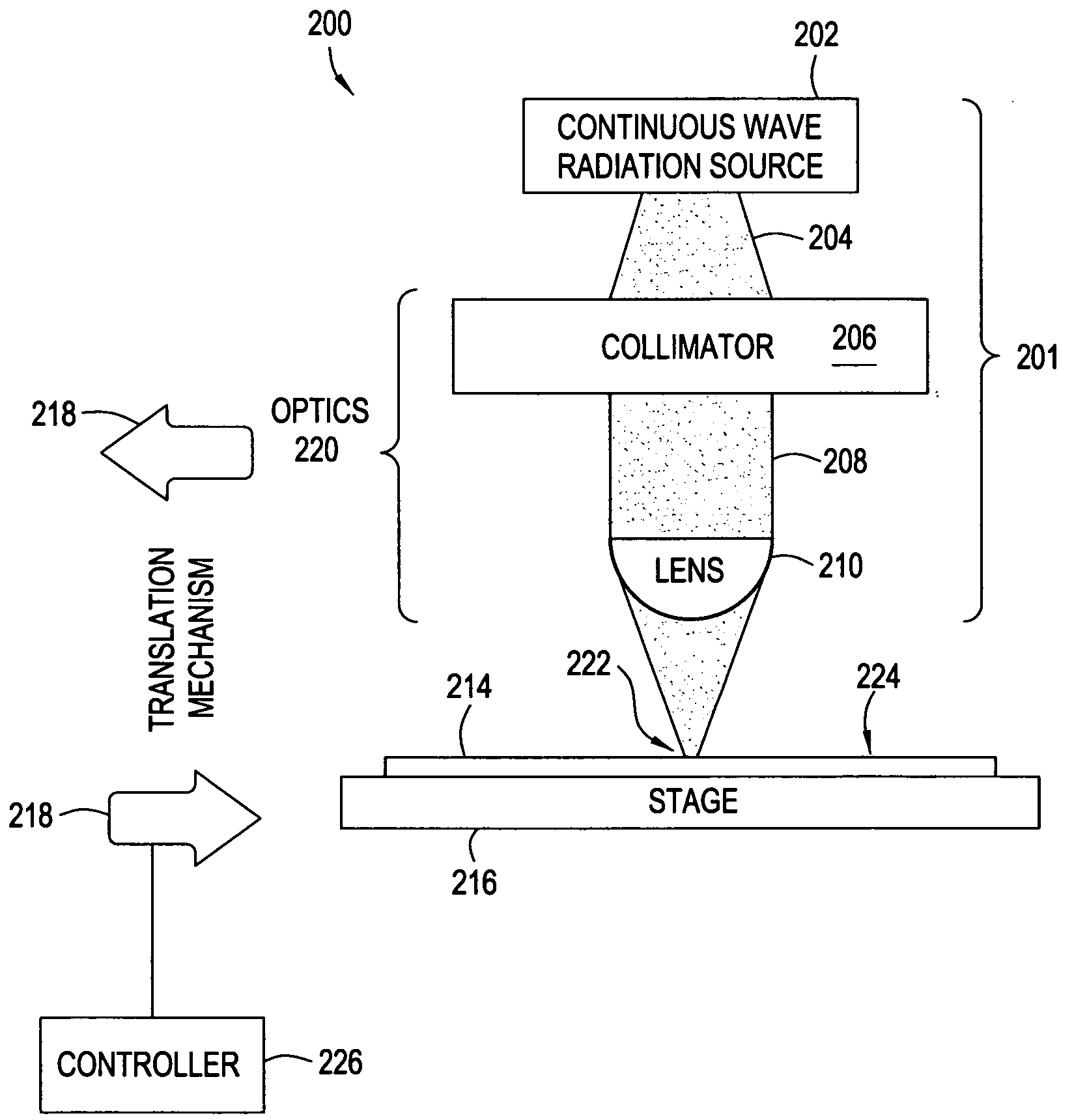
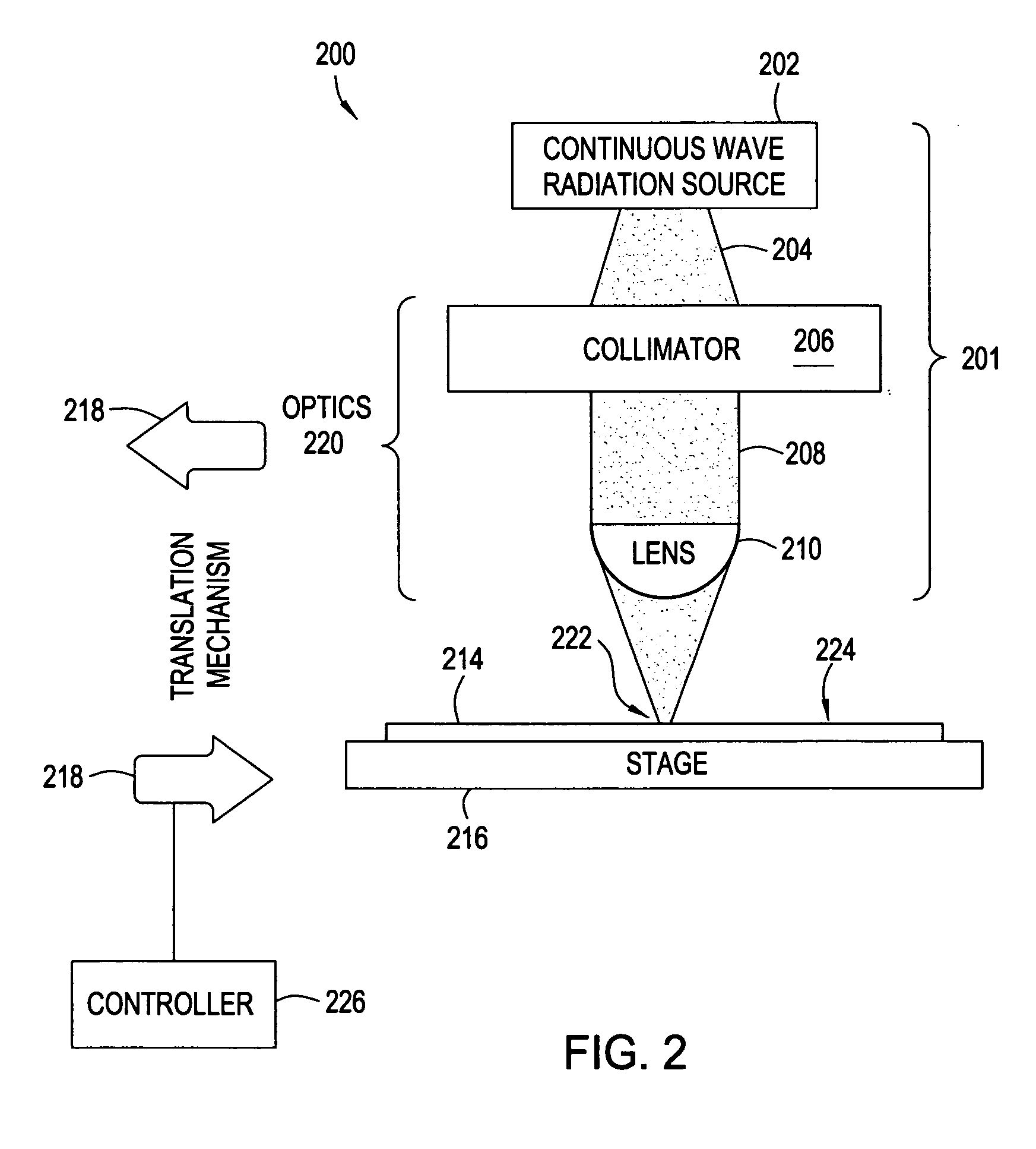
[0041] A layer comprising amorphous carbon was deposited on 9 silicon substrates in a PECVD chamber under the following processing conditions: 550° C., 7 Torr, 700 watts RF power at a frequency of 13.56 MHz, 1200 sccm C3H6, 650 sccm He, and a spacing of 270 mils between the chamber showerhead and the substrate support. The layer was deposited in the absence of a chamber shadow ring in Examples 1-7. The layer was deposited with a chamber shadow ring present in Examples 8 and 9. The substrate was then laser annealed according to embodiments provided herein. The thickness of the deposited layer, deposition time, and the emissivity of the layer to electromagnetic radiation of 810 nm are shown in Table 1.
TABLE 1ApproximateThicknessDepositionSubstrate(Å)EmissivityTime (Sec)19360.896328000.845439000.8961410000.9168511000.9374612000.9481713000.928889000.8734912000.945
examples 10-17
[0042] A layer comprising amorphous carbon and nitrogen was deposited on 8 silicon substrates in a PECVD chamber under the following processing conditions: 400° C. 7 Torr, 1200 watts RF power at a frequency of 13.56 MHz, 350 sccm C3H6, 3400 sccm N2, and a spacing of 270 mils between the chamber showerhead and the substrate support. The layer was deposited was deposited in the absence of a chamber shadow ring in Examples 10-15. The layer was deposited with a chamber shadow ring present in Examples 16 and 17. The substrate was then laser annealed according to embodiments provided herein. The thickness of the deposited layer, deposition time, and the emissivity of the layer to electromagnetic radiation of 810 nm is shown in Table 2.
TABLE 2ApproximateThicknessDepositionSubstrate(Å)EmissivityTime (Sec)108000.9117119000.95191210000.98211311000.99241412000.99261513000.9728168500.94171712000.9825
[0043] As shown in Tables 1 and 2, the layers comprising amorphous carbon and amorphous carbon...
PUM
 Abstract
Description
Claims
Application Information
 - Generate Ideas
- Intellectual Property
- Life Sciences
- Materials
- Tech Scout
- Unparalleled Data Quality
- Higher Quality Content
- 60% Fewer Hallucinations
Browse by: Latest US Patents, China's latest patents, Technical Efficacy Thesaurus, Application Domain, Technology Topic, Popular Technical Reports.
© 2025 PatSnap. All rights reserved.Legal|Privacy policy|Modern Slavery Act Transparency Statement|Sitemap|About US| Contact US: help@patsnap.com