

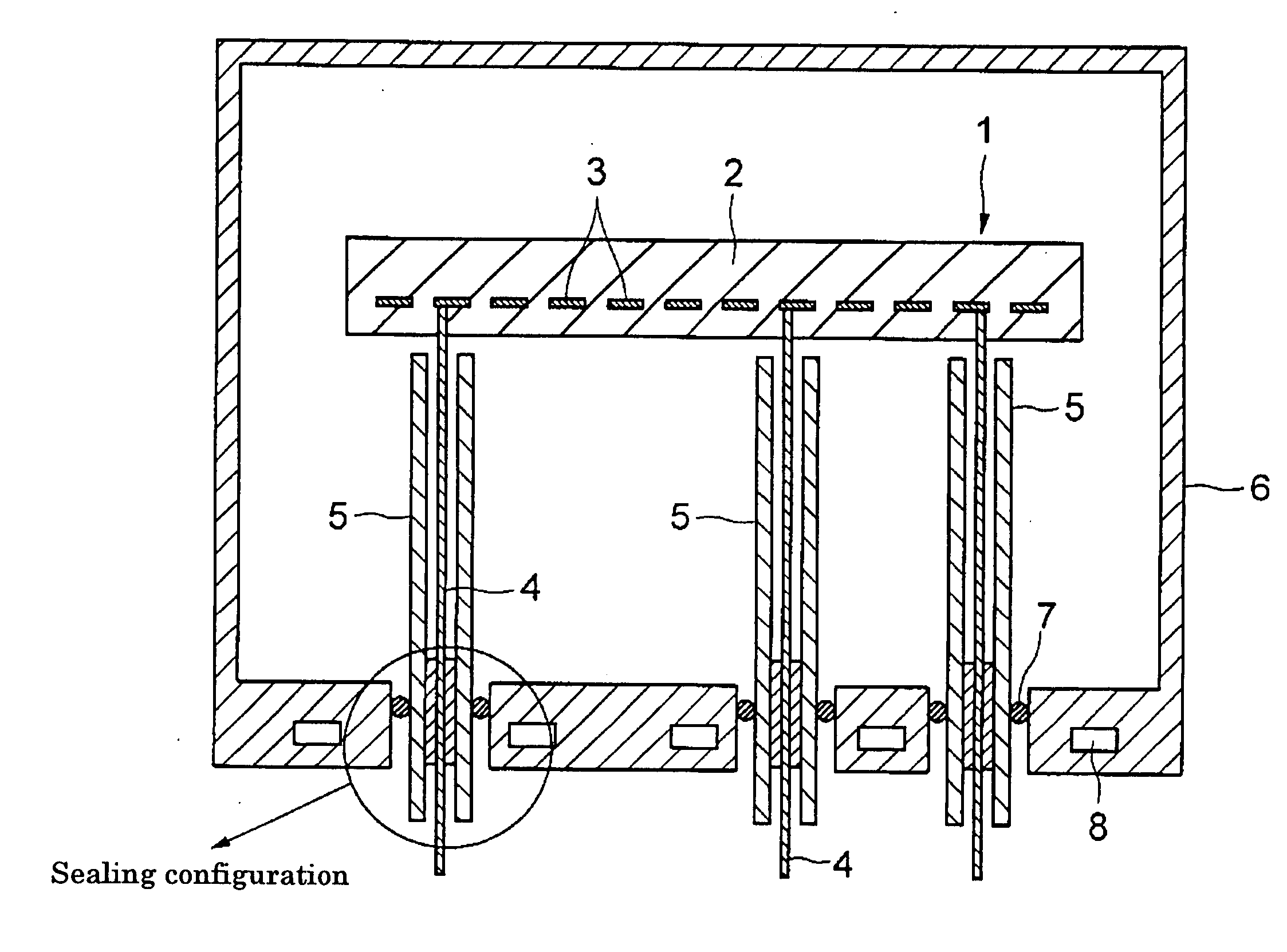
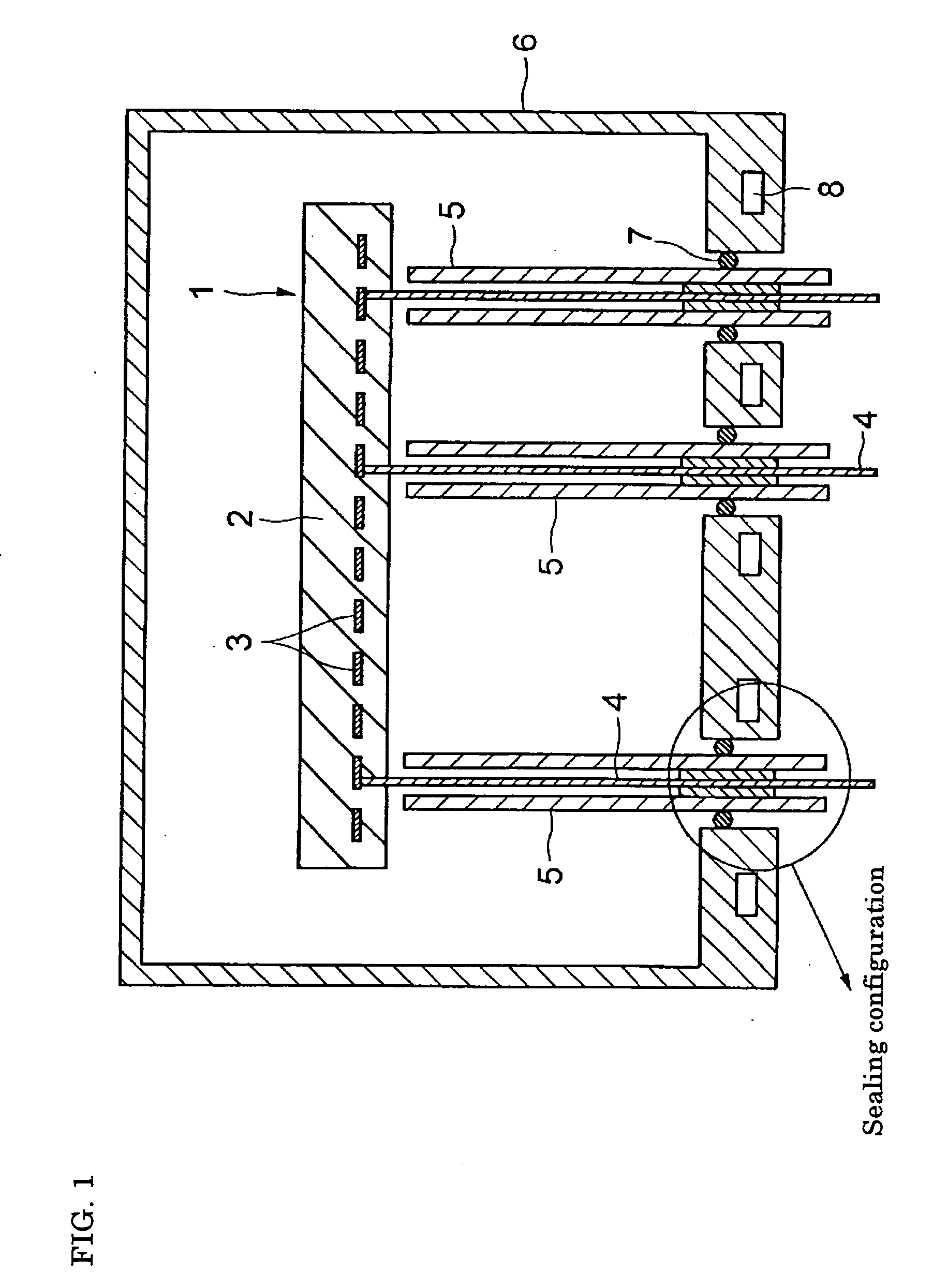
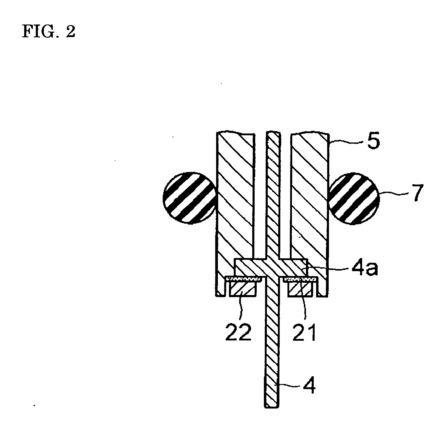
Wafer holder and system for producing semiconductor
a technology of wafer holder and semiconductor, applied in the direction of ohmic resistance heating, hot plate heating arrangement, coating, etc., can solve the problems of reducing temperature, increasing the amount of heat dissipation through the air at atmospheric pressure within the tubular piece, and compromising the temperature uniformity of the wafer support surface, so as to improve the temperature uniformity of the wafer retaining surface
- Summary
- Abstract
- Description
- Claims
- Application Information
AI Technical Summary
Benefits of technology
Problems solved by technology
Method used
Image

Examples
embodiments
Embodiment 1
[0049] Slurries were prepared by adding predetermined amounts of sintering additive, binder, solvent, and so forth to ceramic powders of AlN, Si3N4, Al2O3, and SiC and blending the mixture with a ball mill. These slurries were granulated by spray drying, and the obtained granules were press-molded using dies of predetermined form. The molded objects thus produced were degreased and then sintered at respective predetermined temperatures, and ceramic substrates were obtained.
[0050] Using a technique such as screen printing, a resistive heating element circuit was formed on the ceramic substrates thus obtained, as well as RF electrodes, electrostatic-chuck electrodes, or electron-beam electrodes as needed. Each printed substrate was baked under predetermined conditions, and a ceramic plate was bonded over the substrate to cover the resistive heating element, RF electrodes, and electrostatic-chuck electrodes in order to protect them as needed. A wafer pocket for carrying a...
embodiment 2
[0059] Each sample wafer holder of the present invention fabricated according to Embodiment 1 was installed in a low-k film baking apparatus to process a wafer. The results were that all the wafer holders were capable of performing low-k film baking appropriately, and in particular, the wafer holders that exhibited a temperature uniformity of less than 0.5% yielded excellent film quality.
[0060] Industrial Applicability
[0061] The present invention provides wafer holders in which local heat radiation during heating is kept under control and temperature uniformity of the wafer retaining surface is enhanced. Accordingly, using the wafer holders makes it possible to provide semiconductor manufacturing apparatuses that have high temperature uniformity, superior durability of electrode terminals and leads and are suitable for processing larger-diameter wafers.
PUM
| Property | Measurement | Unit |
|---|---|---|
| inner diameter | aaaaa | aaaaa |
| inner diameter | aaaaa | aaaaa |
| diameter | aaaaa | aaaaa |
Abstract
Description
Claims
Application Information