Solid-state imaging device and method for manufacturing solid-state imaging device
- Summary
- Abstract
- Description
- Claims
- Application Information
AI Technical Summary
Benefits of technology
Problems solved by technology
Method used
Image

Examples
Embodiment Construction
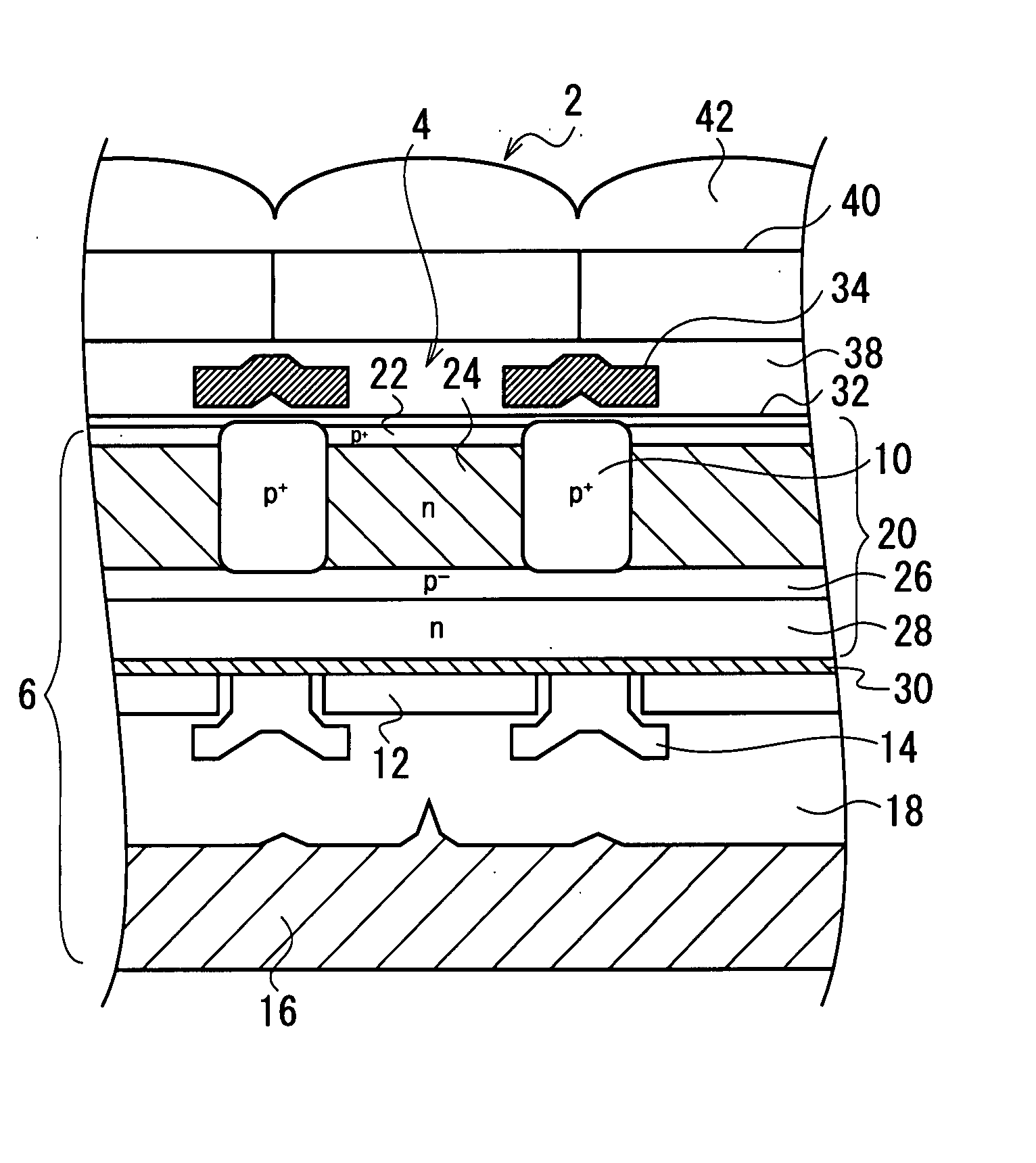
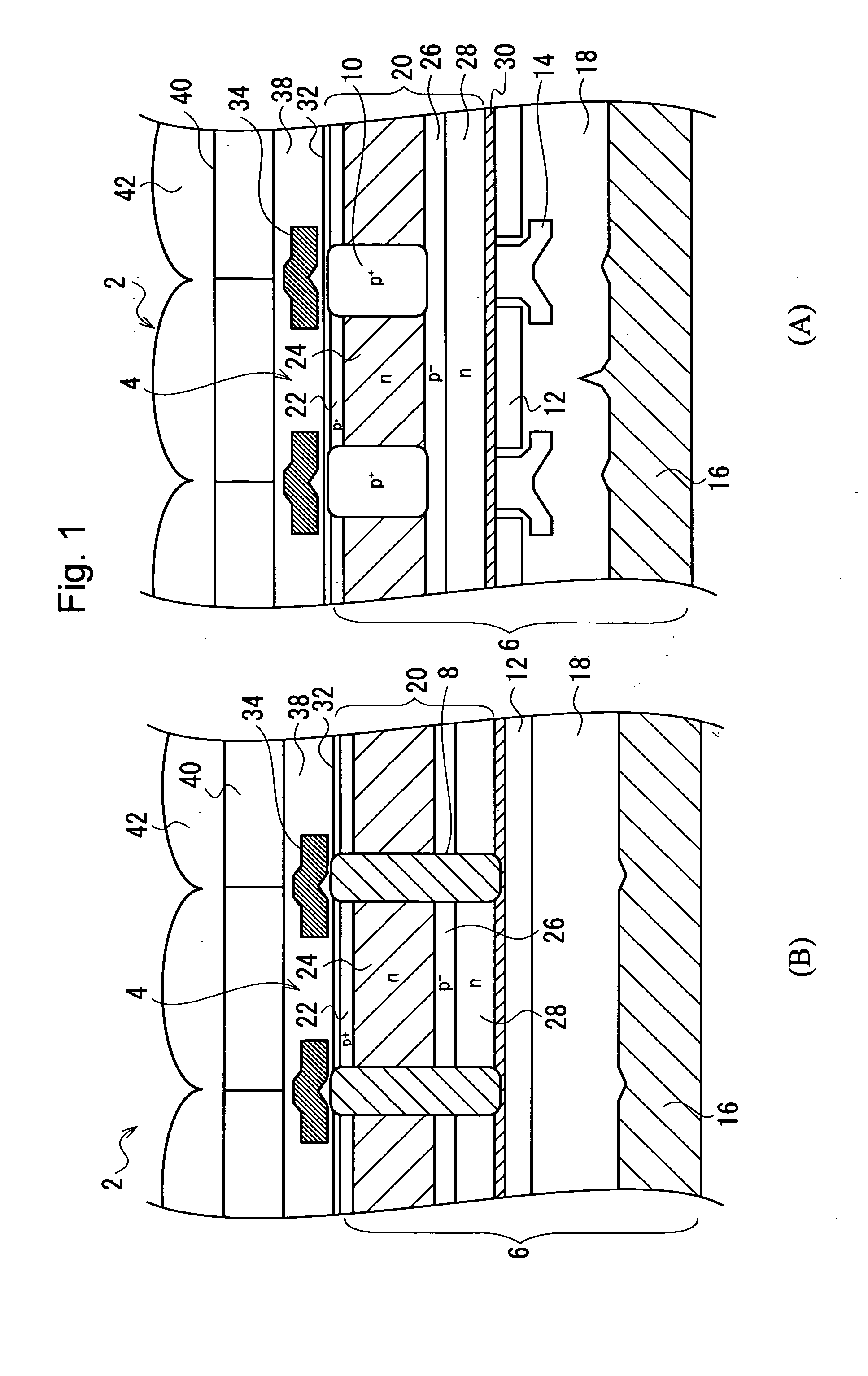
[0018] Next, embodiments of the present invention will be described below with reference to the accompanying drawings.
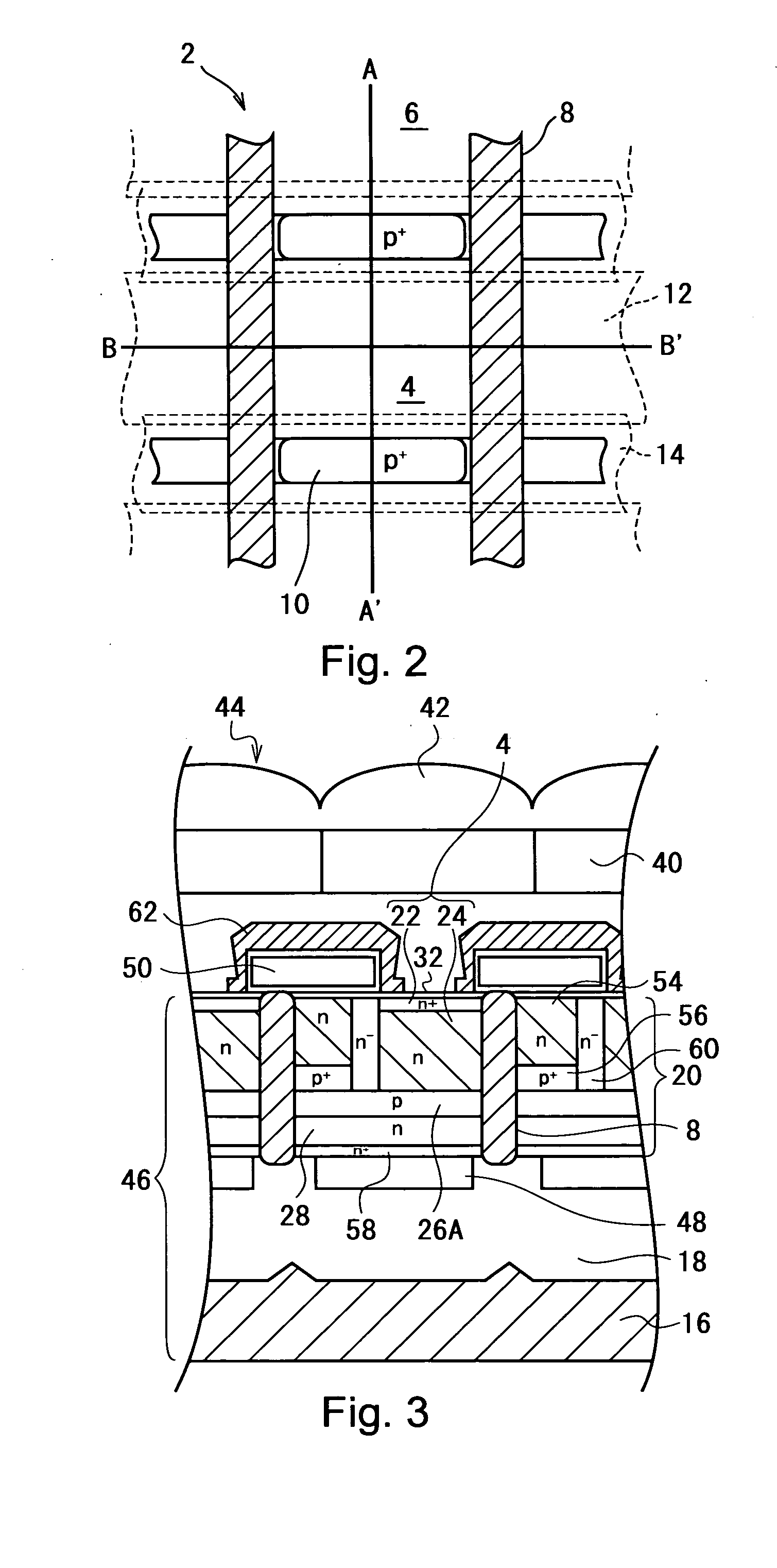
[0019] In FIG. 1, (A) and (B) are sectional side views of a part of a solid-state imaging device according to an embodiment of the present invention, and FIG. 2 is a plan view showing a part of the solid-state imaging device shown in FIG. 1. FIG. 1(A) is a sectional view of FIG. 2 cut along line A-A′, and FIG. 1(B) is a sectional view of FIG. 2 cut along line B-B′.
[0020] As shown in FIG. 2, a solid-state imaging device 2 according to the present embodiment includes a plurality of optical sensors 4 arranged in a surface region of a semiconductor substrate 6 in a matrix pattern such that the optical sensors 4 are adjacent to one another. The optical sensors 4 on each row are separated from one another by device-separating regions 8, as shown also in FIG. 1(B), and the optical sensors 4 on each column are separated from one another by channel-stop regions 10, as shown...
PUM
 Abstract
Description
Claims
Application Information