Array substrate for reflective and transflective liquid crystal display devices and manufacturing method for the same

a liquid crystal display and substrate technology, applied in non-linear optics, instruments, optics, etc., can solve the problems of reducing the electric properties affecting and affecting the stability of liquid crystal panels, so as to improve the contact properties of reflective electrodes.

Inactive Publication Date: 2005-04-14
LG DISPLAY CO LTD
View PDF8 Cites 22 Cited by
  • Summary
  • Abstract
  • Description
  • Claims
  • Application Information

AI Technical Summary

Benefits of technology

[0022] An object of the present invention is to provide an array substrate for a reflective liquid crystal display device, wherein a reflective electrode is not formed on organic insulating material such as benzocyclobutene (BCB), but formed on inorganic insulating material such as silicon nitride (SiNX) to improve contact property of the reflective electrode and to prevent a deposition chamber from being contaminated with particles of the organic insulating material.
[0024] Another object of the present invention is to provide an array substrate for a transflective liquid crystal display device, wherein a reflective electrode is not formed on organic insulating material such as benzocyclobutene (BCB), but formed on inorganic insulating material such as silicon nitride (SiNX) to improve contact property of the reflective electrode and to prevent a deposition chamber from being contaminated with particles of the organic insulating material.
[0026] Another object of the present invention is to provide an array substrate for a transflective liquid crystal display device having a barrier layer between an organic insulating layer and a reflector to improve contact property of the reflective electrode and to prevent a deposition chamber from being contaminated with particles of the organic insulating material.

Problems solved by technology

Because the transflective liquid crystal display device utilizes both of the back light and the external light source, it can save power consumption.
First, because a reflective electrode is formed on an organic insulating layer such as benzocyclobutene (BCB) and the contact property of the reflective electrode and the benzocyclobutene (BCB) layer is not good, the reflective electrode may not be stably deposited on the organic insulating layer.
This lacks of stability lowers electric properties of a liquid crystal panel.
Lastly, an align key may not be detected by a detecting apparatus if the benzocyclobutene (BCB) is deposited on the substrate and covers the align key.
Accordingly, alignment error of a mask and the substrate may be occurred during a light exposing process for patterning the reflective electrode.

Method used


Image

  • Array substrate for reflective and transflective liquid crystal display devices and manufacturing method for the same
  • Array substrate for reflective and transflective liquid crystal display devices and manufacturing method for the same
  • Array substrate for reflective and transflective liquid crystal display devices and manufacturing method for the same

Examples


Embodiment Construction

[0051] Reference will now be made in detail to the preferred embodiment of the present invention, which is illustrated in the accompanying drawings.

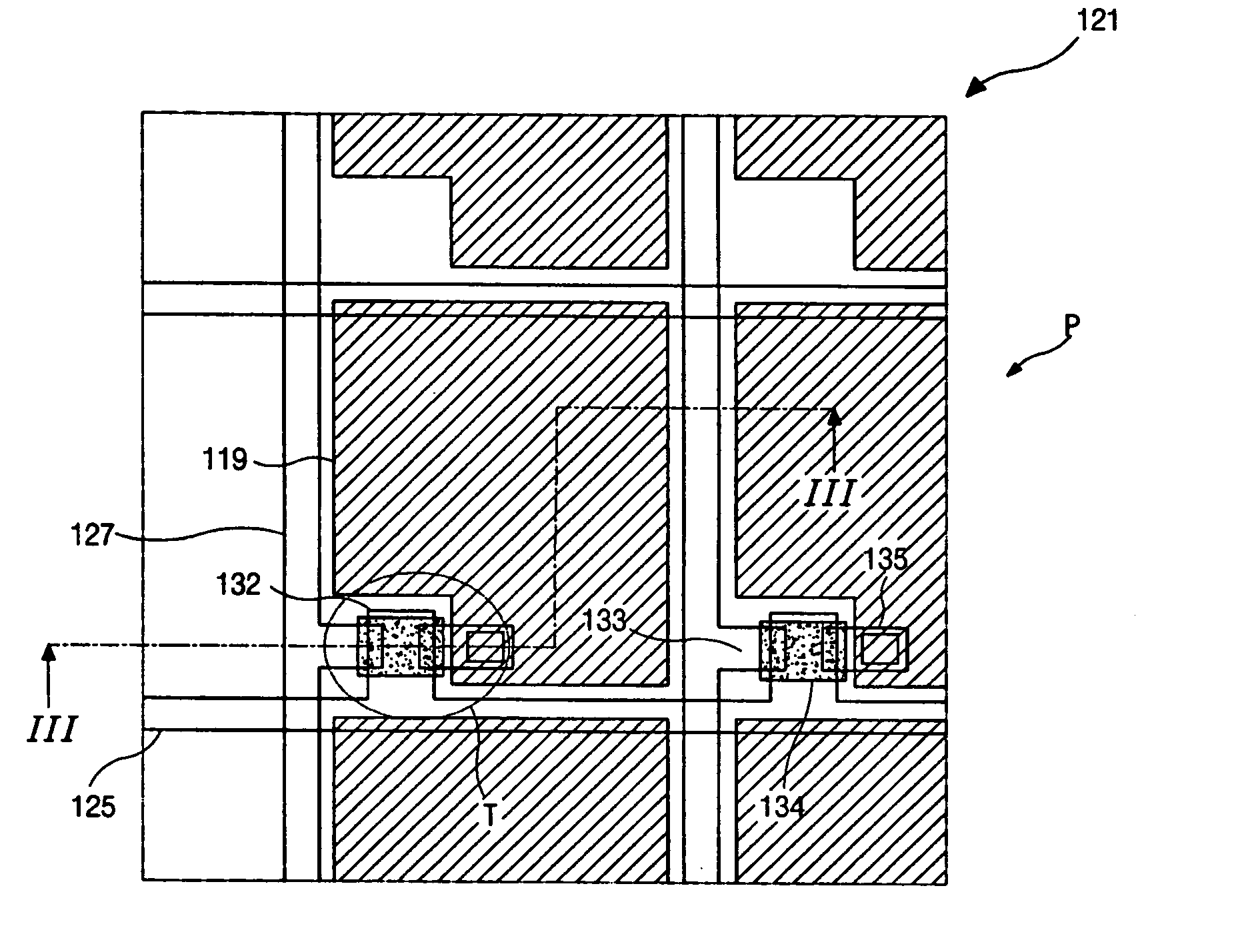
[0052] A first embodiment of the present invention will be described hereinafter with reference to FIG. 8 and FIGS. 9A to 9C. FIG. 8 is a plan view illustrating a partial array substrate for a reflective liquid crystal display device according to the first embodiment of the present invention. FIGS. 9A to 9C are cross-sectional views taken along III-III of FIG. 8 illustrating a fabricating sequence of an array substrate according to the first embodiment of the present invention. In FIG. 9A, a gate line 125 and a gate electrode 132 are formed on the substrate 111 by depositing conductive metal such as aluminum (Al), aluminum alloys, molybdenum (Mo), copper (Cu), tungsten (W) and chromium (Cr), for example, and patterning it. If the gate electrode 132 and the gate line 125 are formed of aluminum (Al), an additional conductive metal layer f...


PUM

PropertyMeasurementUnit
conductiveaaaaaaaaaa
transparentaaaaaaaaaa
insulatingaaaaaaaaaa

Abstract

An array substrate for a reflective liquid crystal display device, including a gate line and a data line defining a pixel region by crossing each other; a switching element at a crossing portion of the gate line and the data line; a first passivation layer covering the switching element and the data line; and formed of an inorganic insulating material; a reflective electrode on the first passivation layer, and connected to the switching element; and a second passivation layer on the reflective electrode. The second passivation layer being formed of an organic insulating material.

Description

[0001] This application is a Divisional of co-pending application Ser. No. 10 / 028,759, filed on Dec. 28, 2001, and for which priority is claimed under 35 U.S.C. § 120; and this application claims priority of Application No. 2001-7097 and 2001-30699 filed in Korea on Feb. 13, 2001 and Jun. 1, 2001, under 35 U.S.C. § 119; the entire contents of all are hereby incorporated by reference.BACKGROUND OF THE INVENTION [0002] 1. Field of the Invention [0003] The present invention relates to liquid crystal display devices, and more particularly, to an array substrate for reflective and transflective liquid crystal display devices. [0004] 2. Description of the Background Art [0005] Generally, a reflective liquid crystal display device does not need to equip an additional light source such as a back light because it can substitute an external light source for the back light. A transflective liquid crystal display device has both properties of the reflective liquid crystal display device and a t...

Claims


Application Information

Patent Timeline
Patent Type & Authority Applications(United States)
IPC IPC(8): G02F1/1335G02F1/1362
CPCG02F1/133553G02F2202/02G02F1/136227G02F1/133555
Inventor PARK, JUNE-HOCHOI, JAE-SIK
Owner LG DISPLAY CO LTD
Why Eureka
Try Eureka