Light-emitting semiconductor device having enhanced brightness

a semiconductor and light-emitting technology, applied in the direction of semiconductor devices, basic electric elements, electrical apparatus, etc., can solve the problems of increasing the time and cost required for movpe epitaxy, poor electric conductivity of algainp or algainn, and significantly increasing the cost of epitaxy, so as to enhance light-emitting efficiency, enhance brightness, and enhance brightness

Inactive Publication Date: 2005-04-21
EPISTAR CORP
View PDF4 Cites 20 Cited by
  • Summary
  • Abstract
  • Description
  • Claims
  • Application Information

AI Technical Summary

Benefits of technology

[0012] It is a primary objective of this invention to provide a light-emitting semiconductor device having enhanced brightness, where width of the meshes of the metallic patterns constructing the front contact ranges from 0.1 to 5 micrometers, thereby enhancing the light-emitting efficiency.
[0013] It is another objective of this invention to provide a light-emitting semiconductor device having enhanced brightness, where the metallic patterns constructing the front contact may be meshed, dotted, checkered or another other geometrical patterns that are evenly distributed above the entire active layer.
[0014] It is a further objective of this invention is to provide a light-emitting semiconductor device having enhanced brightness, where the metallic patterns constructing the front contact does not mask the light illuminated by the active layer because the width of the metallic patterns is less than 5 micrometers.
[0015] To achieve the above objectives, this invention adopts the method comprising the steps of: forming an active layer on a substrate; forming a capping layer on the active layer to enhance current distribution, where a back contact is located on another side of the substrate and a front contact is located above the capping layer. This invention is characterized in that, the front contact is re-designed to reduce the width of metallic patterns constructing fingers or Mesh lines and to increase the number of the fingers or Mesh lines, so as to resolve the current crowding problem. When the metallic patterns are dimensioned to be 2 micrometers, even the light emitted by the active layer that is exactly located below the metal is still visible through the capping layer at a light-emitting angle of 3.8 to 18 degrees, whereby current concentration may be enhanced to improve the light-emitting efficiency.

Problems solved by technology

However, the low carrier mobility and high resistance of the active layer made of AlGaInP or AlGaInN results in poor electric conductivity of the AlGaInP or AlGaInN.
As described in the '718 patent, to improve the current distribution, the capping layer is preferred to be in the range from 150 to 200 micrometers thick to enhance the luminous intensity by 5 to 10 times. However, the increasing thickness of the capping layer also increases the time and cost required for MOVPE epitaxy thereby significantly increasing the cost of the epitaxy.
Hence, to ensure even current distribution, the thickness must be at least 10 micrometers or the current crowding problem cannot be effectively resolved.
The result, however, is not satisfactory because the inherent width of the Mesh lines extending from the contacts usually ranges from 5 to 25 micrometers to ensure easy production.
Since the current located exactly below the contacts are most intensive to result in intensive illumination, the metal meshes mask the regions that are intensively illuminated.
However, reducing the number the metal meshes will cause poor current distribution at some of the luminous regions E so as to affect the light-emitting effects (as shown in FIGS. 1G to 1H).

Method used


Image

  • Light-emitting semiconductor device having enhanced brightness
  • Light-emitting semiconductor device having enhanced brightness
  • Light-emitting semiconductor device having enhanced brightness

Examples


example i

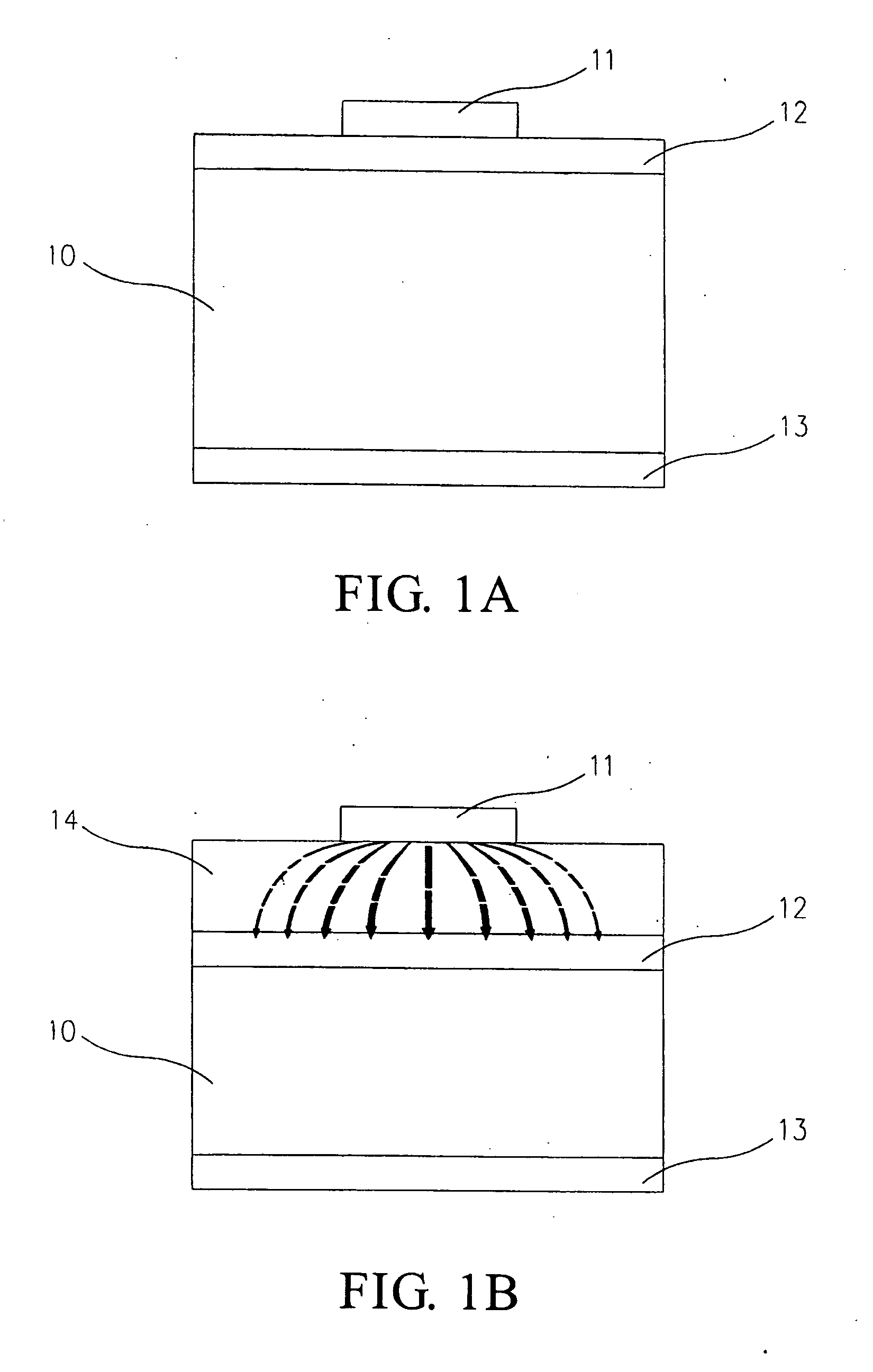
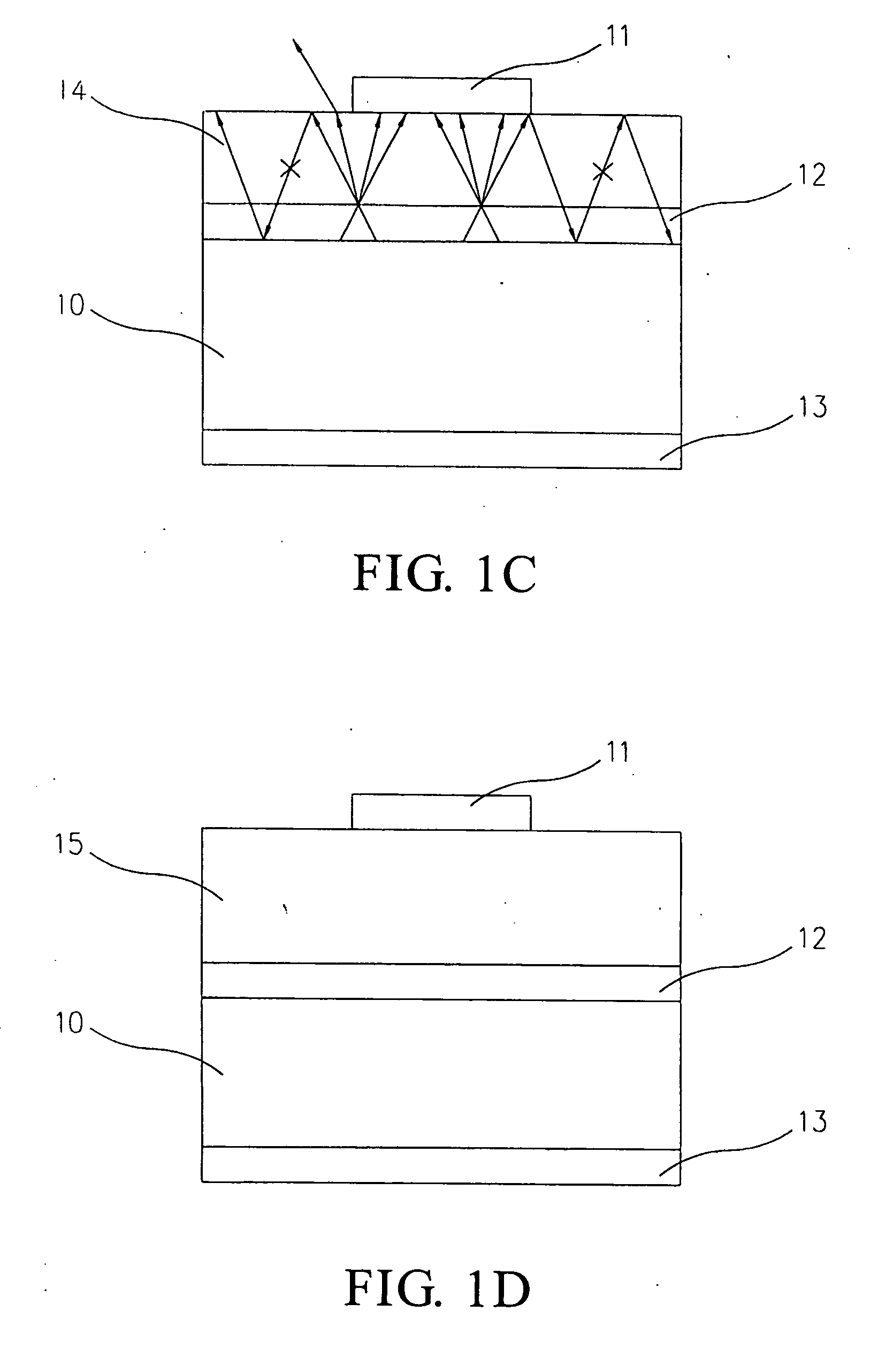
[0031] In Example I, a light emitting diodes (LED) is used to describe the features of this invention. FIG. 2A is a cross-sectional view of a light emitting diode. First, an active layer 120 is formed above a substrate 100. The active layer may be of a double-heterostructure or a quantum well structure to enhance the light-emitting efficiency of the diode. Then, a capping layer 140 made of GaP, AlGaAs or ITO is then added above the active layer to increase the current distribution. A back contact 130 is located on another side of the substrate 100, and a front contact 210 is located above the capping layer 140.

[0032] In detail, the material of the substrate 100 is dependent on the material of the active layer 120. When the active layer 120 is made of AlGaInP, GaAs is selected to form the substrate. When the active layer 120 is made of AlGaInN. Any of sapphire, SiC, MgAlO4, ZnO, LiG2O2 and LiAlO2 may be selected to form the substrate. The active layer is preferred to be in the range...

example ii

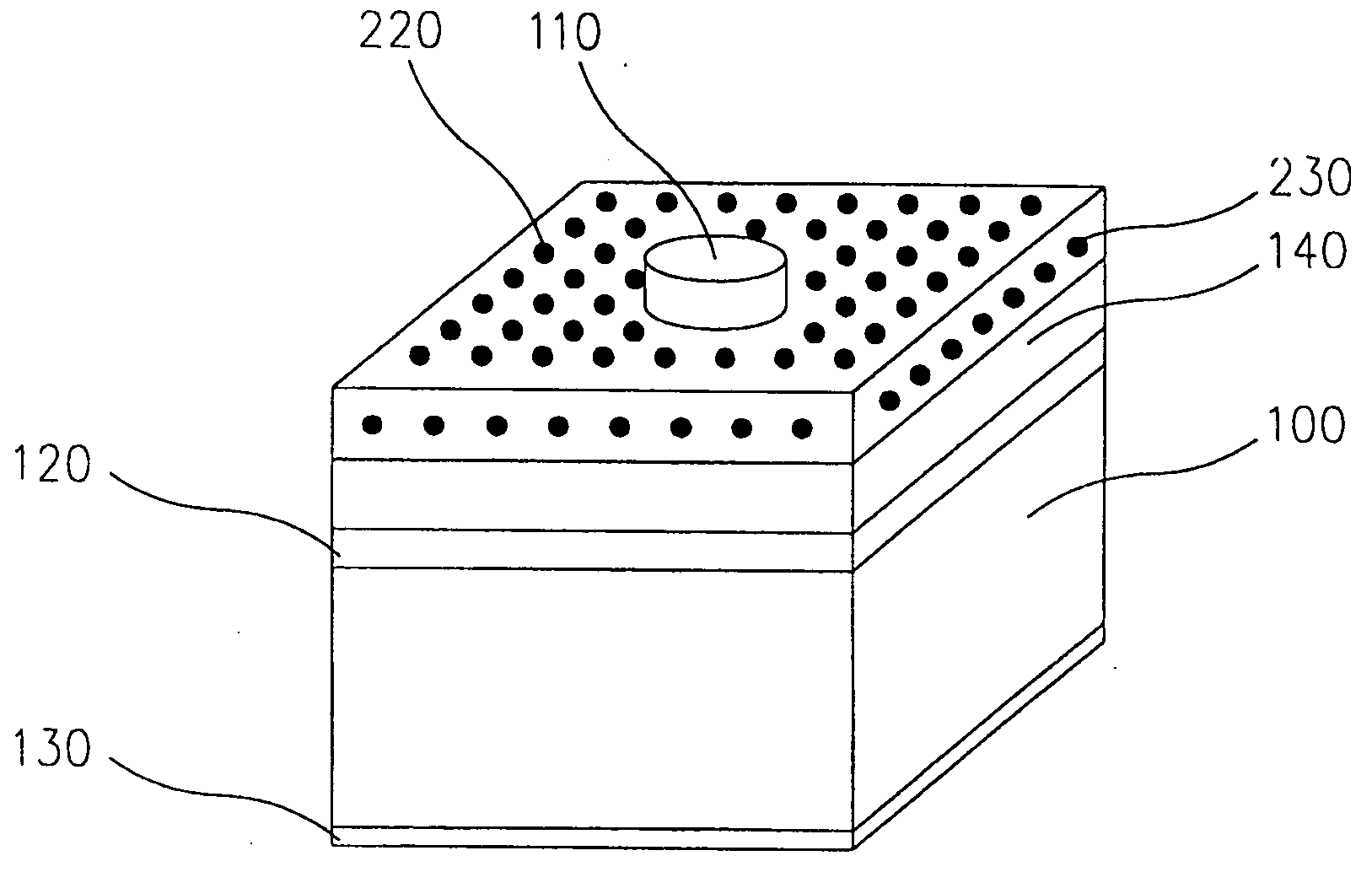
[0042] Example II discloses a further light emitting diodes (LED) to describe the features of this invention. FIG. 2D is a cross-sectional view of a light emitting diode, having a back contact, a substrate, an active layer and a capping layer that have the same structures as those in Example I. According to this invention, the substrate may a semiconductor substrate or any other appropriate substrates dependent on the applications of the LED.

[0043] Example II is characterized by a front contact that is divided into two layers, as shown in FIG. 2E. The metallic bonding pad—a first layer 110 of the front contact, is the same as that adopted in the conventional light emitting diodes. The contact is located at a center of the diode to serve as the media for communicating and contacting the exterior. A second layer 220 of the front contact is located below the first layer 110 and embedded in an ITO layer 230. The second layer 220 of the front contact includes a metallic pattern having a...


PUM


Abstract

This invention this invention provides a light-emitting semiconductor device having enhanced brightness, to ensure even current distribution emitted by a front contact of the light emitting diodes so as to improve the light-emitting efficiency of the active layer. This invention adopts the method to manufacture the light-emitting device, comprising the steps of: forming an active layer on a substrate; forming a capping layer on the active layer to enhance current distribution, where a back contact is located on another side of the substrate and a front contact is located above the capping layer. This invention is characterized by: re-designing the front contact, by reducing the width of a metallic pattern constructing fingers or Mesh lines and increasing the number of the fingers or Mesh lines, so as to resolve the current crowding problem.

Description

CROSS-REFERENCES TO RELATED APPLICATIONS [0001] Not Applicable STATEMENT REGARDING FEDERALLY SPONSORED RESEARCH OR DEVELOPMENT [0002] Not Applicable DESCRIPTION [0003] 1. Field of Invention [0004] This invention relates to a light-emitting semiconductor device having enhanced brightness, particularly to one for enhancing current distribution of a front contact in a light emitting diode, so as to enhance the light emitting efficiency of a light-emitting semiconductor. [0005] 2. Background [0006] The principles lying behind luminance of light emitting diodes relate to passing current sequentially through P-N junctions of a semiconductor to generate light, wherein AlGaInP is implemented in high brightness red, orange, yellow and yellowish green LEDs, AlGaInN is in blue and green LEDs. The process of metal organic vapor phase epitaxy (MOVPE) is commonly adopted in the mass production of the LEDs, while the light-emitting components are of the structures, including: homo-junction (HOMO),...

Claims


Application Information

Patent Timeline
Patent Type & Authority Applications(United States)
IPC IPC(8): H01L29/205H01L33/38H01L33/42
CPCH01L33/38H01L33/42H01L33/387
Inventor CHIEN, WEI-ENCHANG, CHIH-SUNGTZER-PERNG, CHEN
Owner EPISTAR CORP
Why Eureka
Try Eureka