MIM capacitor structure and method of manufacture

a technology of metal-insulator metal and capacitor, which is applied in the direction of capacitors, semiconductor devices, electrical equipment, etc., can solve the problems of insufficient overlap margin, difficult to fill the narrow, deep contact patterns of conductive materials with conductive materials, and difficulty in combining capacitor manufacturing, so as to improve the overlay process margin and increase the capacitance

Active Publication Date: 2005-04-21
TAIWAN SEMICON MFG CO LTD
View PDF12 Cites 84 Cited by
  • Summary
  • Abstract
  • Description
  • Claims
  • Application Information

AI Technical Summary

Benefits of technology

[0014] Advantages of embodiments of the present invention include providing a method of forming MIM capacitors that is absent the bitline contact to top plate electrode shorting that is found in prior art MIM capacitor manufacturing methods. Capacitors with increased capacitance for a given layout area may be manufactured

Problems solved by technology

It is challenging to merge the manufacturing of capacitors 102 in DRAM regions with logic circuits in the logic region.
These high aspect ratio contacts 126 are problematic because the contact pattern is difficult to etch through the thicknesses of the dielectric layers 124, 116, 114 and 110, and also because it is diffic

Method used


Image

  • MIM capacitor structure and method of manufacture
  • MIM capacitor structure and method of manufacture
  • MIM capacitor structure and method of manufacture

Examples


first embodiment

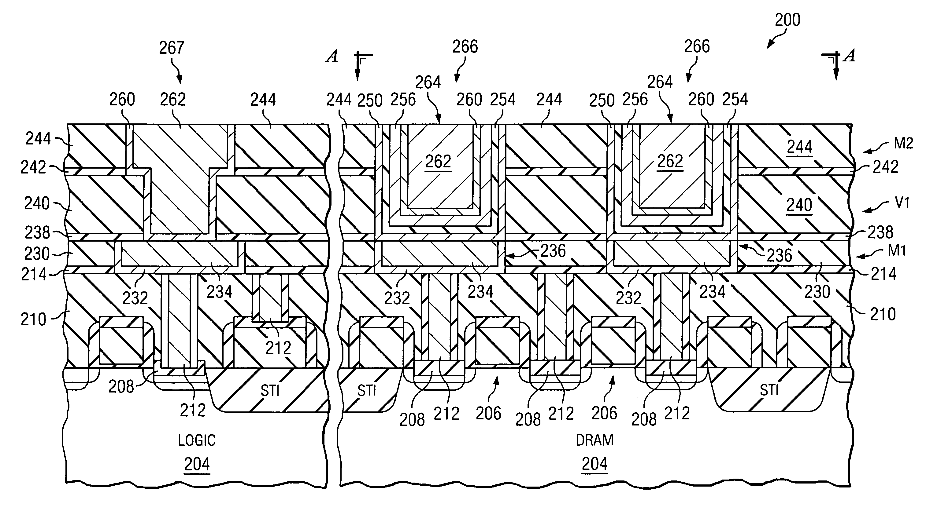
[0052] The MIM capacitors 376 comprise a bottom plate 378 that includes the first conductive barrier layer 332, first conductive material 334, second conductive barrier layer 360, second conductive material 362, and conductive material layer 350. The MIM capacitors 376 also include a top plate 380 that comprises the top plate electrode material 356, the third conductive barrier layer 382 and the third conductive material 384. A conductive plug 386 is formed in the logic region that extends through the metallization layers M1, M2 and M3, and the via layers V1 and V2, as shown. Advantageously, in this embodiment, a portion of the top or sixth insulating layer 332 may also be removed, providing connections between adjacent MIM capacitors, as shown in FIG. 6. FIG. 6 shows a cross-sectional view of the semiconductor device 300 shown in FIG. 5, rotated by 90 degrees in the DRAM region. As in the first embodiment, a top portion of the sixth insulating layer 372 is recessed by an amount d2 ...

third embodiment

[0054] the present invention is shown in a cross-sectional view in FIG. 7. In this embodiment, again, a portion of the bottom electrode 490 of the MIM capacitors 488 are formed in the first metallization layer M1. However, in this embodiment, the MIM capacitors 488 are formed in three or more of the insulating layers 440, 444, 468, and 472. For example, the MIM capacitors 488 are formed in the third insulating layer 440, the fourth insulating layer 444, the fifth insulating layer 468, and the sixth insulating layer 472. Note that the MIM capacitors 488 are also formed in the respective stop layers, which include second stop layer 438, third stop layer 442, fourth stop layer 446, and fifth stop layer 470. A sixth stop layer may also be used over the top surface of the sixth insulating layer 472, not shown.

[0055] In this embodiment, prior to filling the third metallization layer M3 and the second via layer V2 with a conductive barrier layer 482 and a conductive material 484, the MIM c...


PUM


Abstract

A metal-insulator-metal (MIM) capacitor structure and method of manufacturing thereof. A plurality of MIM capacitor patterns is formed in two or more insulating layers. The insulating layers may comprise a via layer and a metallization layer of a semiconductor device. A top portion of the top insulating layer is recessed in a region between at least two adjacent MIM capacitor patterns. When the top plate material of the MIM capacitors is deposited, the top plate material fills the recessed area of the top insulating layer between the adjacent MIM capacitor pattern, forming a connecting region that couples together the top plates of the adjacent MIM capacitors. A portion of the MIM capacitor bottom electrode may be formed in a first metallization layer of the semiconductor device.

Description

TECHNICAL FIELD [0001] Embodiments of the present invention relate generally to the fabrication of semiconductor devices, and more particularly to the fabrication of metal-insulator-metal (MIM) capacitors. BACKGROUND [0002] Capacitors are elements that are used extensively in semiconductor devices for storing an electrical charge. Capacitors essentially comprise two conductive plates separated by an insulator. The capacitance, or amount of charge held by the capacitor per applied voltage, depends on a number of parameters such as the area of the plates, the distance between the plates, and the dielectric constant value for the insulator between the plates, as examples. Capacitors are used in filters, analog-to-digital converters, memory devices, control applications, and many other types of semiconductor devices. [0003] One type of capacitor is a MIM capacitor, which is frequently used in mixed signal devices and logic devices, as examples. MIM capacitors are used to store a charge ...

Claims


Application Information

Patent Timeline
IPC IPC(8): H01L21/02H01L21/8242
CPCH01L27/10852H01L27/10855H01L28/91H01L28/60H01L27/10894H10B12/09H10B12/033H10B12/0335
Inventor TU, KUO-CHICHEN, CHUN-YAOWUU, SHOU-GWOWANG, CHEN-JONG
Owner TAIWAN SEMICON MFG CO LTD
Why Eureka
Try Eureka