Semiconductor laser module, optical amplifier, and method of manufacturing the semiconductor laser module

a laser module and semiconductor technology, applied in the direction of semiconductor lasers, instruments, optical elements, etc., can solve the problems of increasing the degree of polarization and high cost, and achieve the effect of shortening the time period

Inactive Publication Date: 2005-04-21
FURUKAWA ELECTRIC CO LTD
View PDF5 Cites 41 Cited by
  • Summary
  • Abstract
  • Description
  • Claims
  • Application Information

AI Technical Summary

Benefits of technology

[0061] According to the thus structured semiconductor laser module manufacturing method, depolarized laser light can be obtained from the optical fiber. Furth...

Problems solved by technology

Another problem of Prior Art 1 is high cost because a long polarization maintaining fiber has to be used in order to lower the degree of polarization satisfactorily.
Furthe...

Method used


Image

  • Semiconductor laser module, optical amplifier, and method of manufacturing the semiconductor laser module
  • Semiconductor laser module, optical amplifier, and method of manufacturing the semiconductor laser module
  • Semiconductor laser module, optical amplifier, and method of manufacturing the semiconductor laser module

Examples


first embodiment

[0092] (First Embodiment)

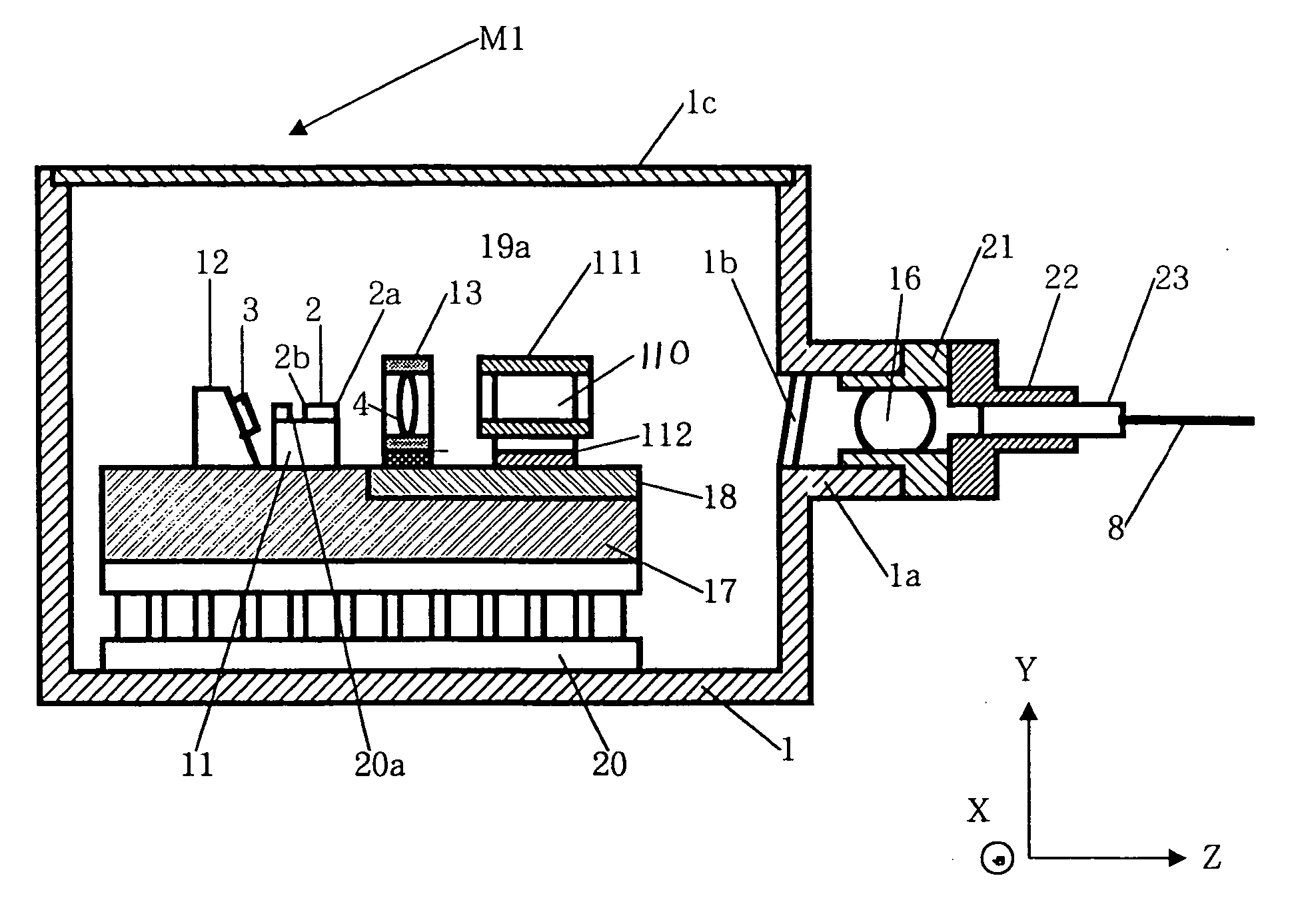
[0093]FIG. 1 is a side sectional view showing a structure of a semiconductor laser module M1 according to a first embodiment of the present invention.

[0094] As shown in FIG. 1, a semiconductor laser module M1 according to the first embodiment of the present invention includes a package 1 whose interior is hermetically sealed, a semiconductor laser device 2 which has a stripe-shaped active layer (hereinafter referred to as stripe) for emitting laser beams and which is encased in the package 1, a photodiode (a light receiving element) 3, a first lens 4, a depolarizing element 110, and an optical fiber 8.

[0095] The semiconductor laser device 2 is fixedly attached on to a chip carrier 11.

[0096] The photodiode 3 receives monitoring laser beam emitted from an end face 2b on a rear side (left side in FIG. 1) of the stripe of the semiconductor laser device 2. The photodiode 3 is fixedly attached to a photodiode carrier 12.

[0097] The first lens 4 is a collimating...

second embodiment

[0111] (Second Embodiment)

[0112]FIG. 3 is a side sectional view showing a structure of a semiconductor laser module M2 according to a second embodiment of the present invention.

[0113] As shown in FIG. 3, the semiconductor laser module M2 according to the second embodiment of the present invention is characterized in that a holder member 111 holding a depolarizing element 110 is fixed to an end of a flange portion 1a formed in a side of a package 1, and that a second lens holding member 21 holding a second lens 16 for collecting laser light that has exited the depolarizing element 110 is fixed to the holder member 111.

[0114] A ferrule 23 holding an optical fiber 8 through a metal slide ring 22 is fixed to an end of the second lens holding member 21 by YAG laser welding.

[0115] Described next is a method of manufacturing the semiconductor laser module M2 according to the second embodiment of the present invention.

[0116] First, a chip carrier 11 with a semiconductor laser device 2 f...

third embodiment

[0125] (Third Embodiment)

[0126]FIG. 4 is a side sectional view showing a structure of a semiconductor laser module M3 according to a third embodiment of the present invention.

[0127] As shown in FIG. 4, the semiconductor laser module M3 according to the third embodiment of the present invention is characterized in that a holder member 111 holding a depolarizing element 110 is fixed to a rear end of a first lens holding member 13 holding a first lens 4.

[0128] A base to which a semiconductor laser device 2 and the first lens 4 are to be fixed is roughly shaped like the letter L by fixing a second base 18 to an end of a first base 17 by silver alloy brazing. The first base 17 is flat and made of CuW. The second base 18 is made of stainless steel and has an opening 18a. The semiconductor laser device 2 is fixed to the first base 17 whereas the first lens holding member 13 is fit into the opening 18a of the second base 18 and is fixed along the perimeter of the opening 18a to the second...


PUM


Abstract

A semiconductor laser module has a semiconductor laser device; a package for housing the semiconductor laser device; a PBC fixed in the package for polarization-synthesizing two laser beams output from the semiconductor laser device; a depolarizing element fixed in the package for depolarizing a synthesizing light output from the PBC; and an optical fiber for receiving a light output from the depolarizing element.

Description

BACKGROUND [0001] (1) Technical Field [0002] The present invention relates to a semiconductor laser module, a Raman amplifier, and a method of manufacturing the semiconductor laser module, and more specifically to a semiconductor laser module in which laser light emitted from a semiconductor laser device is coupled to an optical fiber, a Raman amplifier, and a method of manufacturing the semiconductor laser module. [0003] (2) Description of Related Art [0004] With progress in the optical communications based on a dense wavelength division multiplexing transmission system over the recent years, a higher output is increasingly demanded to a pumping light source used for the optical amplifier. [0005] Further, a greater expectation is recently given to a Raman amplifier as an amplifier for amplifying the light having a much broader band than by an EDFA (erbium-doped optical fiber amplifier) that has hitherto been employed as the optical amplifier. The Raman amplifier may be defined as a...

Claims


Application Information

Patent Timeline
IPC IPC(8): G02B6/34G02B6/42H01S3/094H01S3/30H01S5/00H01S5/02H01S5/022H01S5/024H01S5/0683H01S5/10H01S5/12H01S5/125H01S5/223H01S5/227H01S5/34H01S5/343H01S5/40
CPCB82Y20/00H01S5/4087G02B6/4201G02B6/4204G02B6/4237G02B6/4248H01S3/094003H01S3/094073H01S3/302H01S5/005H01S5/02248H01S5/02284H01S5/02415H01S5/0683H01S5/1039H01S5/1203H01S5/125H01S5/2231H01S5/227H01S5/3409H01S5/34373H01S5/4012H01S5/4031G02B6/2786G02B6/4271H01S5/02251H01S5/02325
Inventor NAKAE, MASASHIAIKIYO, TAKESHIKIMURA, TOSHIO
Owner FURUKAWA ELECTRIC CO LTD
Why Eureka
Try Eureka