

Method and system for reparing defected photomasks
a photomask and defect technology, applied in the field of photomask repair, can solve the problems of high equipment cost, high system complexity, and non-uniformity in some mask steps, such as the diameter of contact holes, and achieve the effect of reducing equipment cost and reducing equipment maintenance costs
- Summary
- Abstract
- Description
- Claims
- Application Information
AI Technical Summary
Benefits of technology
Problems solved by technology
Method used
Image

Examples
Embodiment Construction
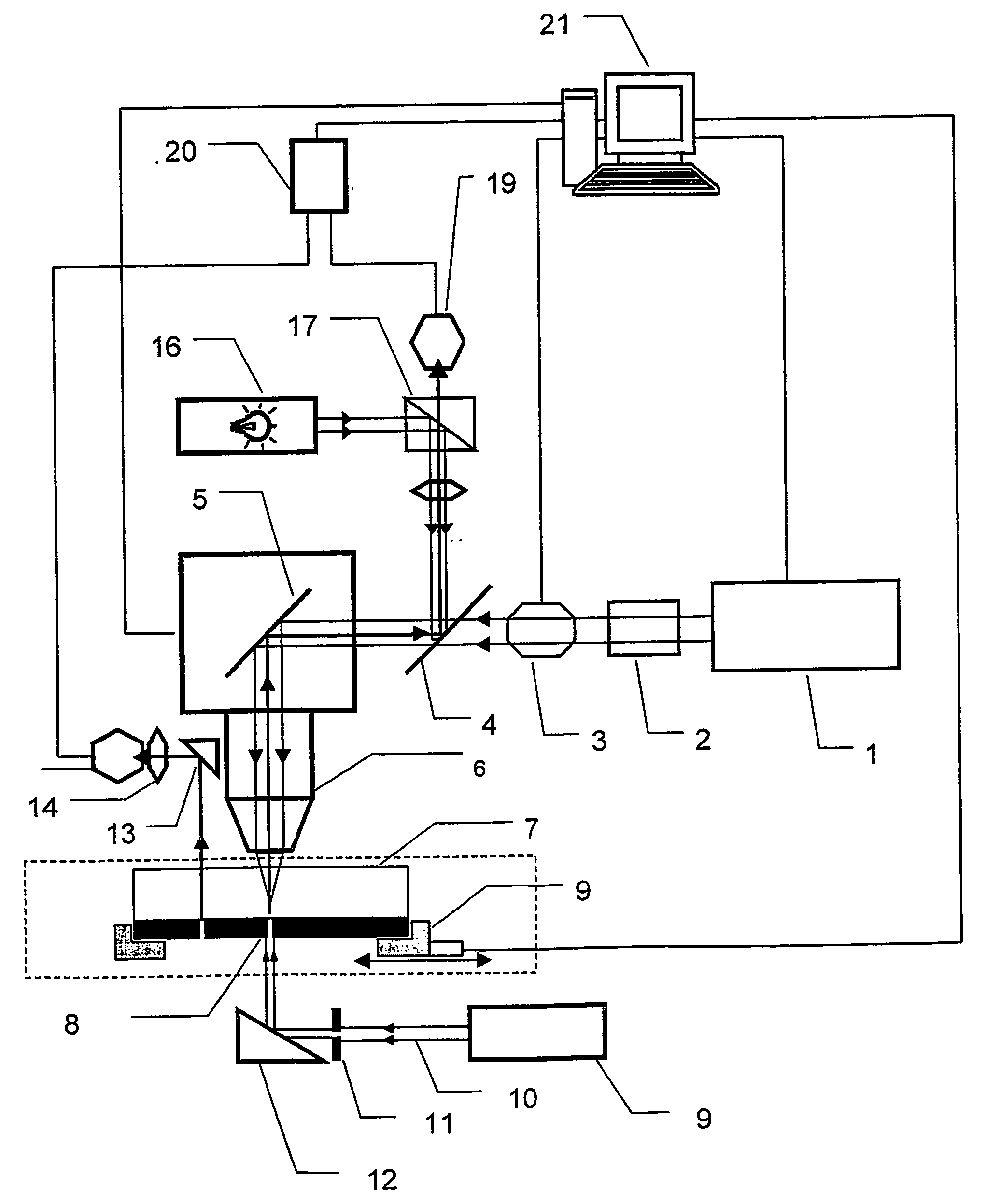
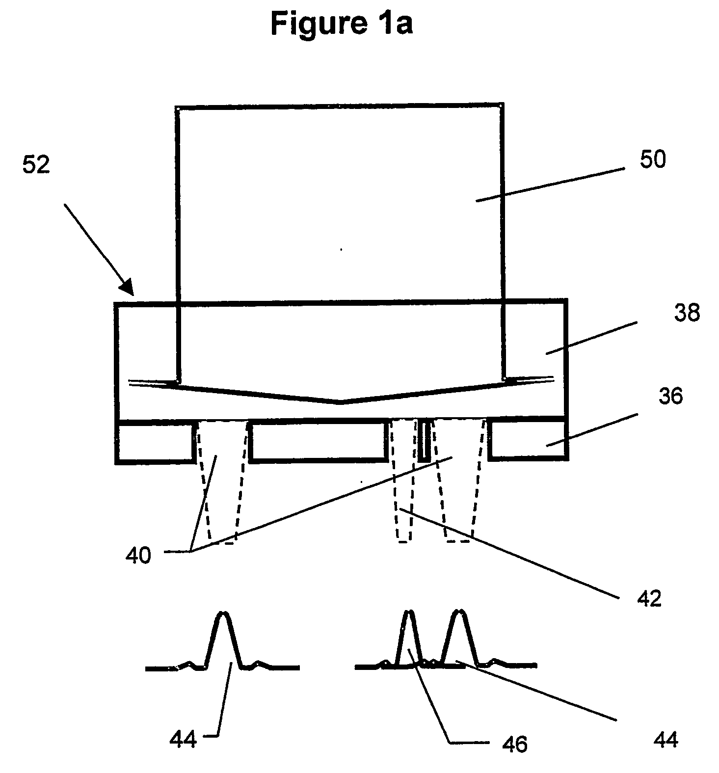
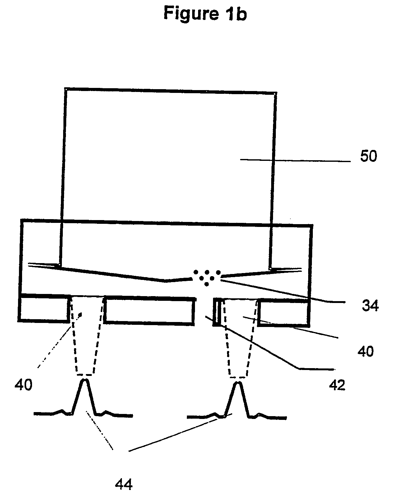
[0061] An aspect of the present invention is repairing a damaged photomask—mask with undesired defect, be it due to a scratch, hole, lack of material, excessive material or other unintentional reason, in the chrome layer (other than the desired pattern)—by writing a diffractive optical element (DOE) or a shading element (SE) in front of the undesired defect. This serves to effectively block, diffract or divert light irradiation as the mask is irradiated in the IC manufacturing process. This way the irradiated light in the IC manufacturing process is redistributed to overcome the defect, so that the desired pattern is printed correctly onto the wafer. The DOE / SE structure design is aimed at casting a shadow or change the scattering properties of the substrate adjacent a void or pin-hole scratches, or any other defect in Chrome layer of the photo masks. Throughout this specification, the term “DOE” (diffractive optical element) means all types of diffractive elements and also includes...
PUM
| Property | Measurement | Unit |
|---|---|---|
| wavelength | aaaaa | aaaaa |
| wavelengths | aaaaa | aaaaa |
| wavelengths | aaaaa | aaaaa |
Abstract
Description
Claims
Application Information