Method for fabricating NROM memory cells with trench transistors

a technology of trench transistors and memory cells, applied in the field of methods, can solve the problems of small nonvolatile memory cells, inability to achieve large storage capacities in the context of conventional fabrication technologies, and the channel length of memory transistors cannot be significantly less than 200 nm, and achieve good electrical junction

Inactive Publication Date: 2005-04-21
POLARIS INNOVATIONS
View PDF11 Cites 5 Cited by
  • Summary
  • Abstract
  • Description
  • Claims
  • Application Information

AI Technical Summary

Benefits of technology

[0011] If no separate etching stop layer is used, the critical position of the top side of the semiconductor material results during the etching of the bit lines. In this case, the depth of the position of the junctions is subsequently set by means of a separately introduced implantation of dopant, which finally forms the source/drain regions. If the implants for the source/drain regions have already been introduced before the fabrication of the bit lines, what is achieved by an etching stop layer is that the original top side of the semiconductor material remai

Problems solved by technology

Extremely small nonvolatile memory cells are required for very large scale integration density in multimedia applications.
The further development of semiconductor technology is enabling increasingly larger sto

Method used


Image

  • Method for fabricating NROM memory cells with trench transistors
  • Method for fabricating NROM memory cells with trench transistors
  • Method for fabricating NROM memory cells with trench transistors

Examples


Embodiment Construction

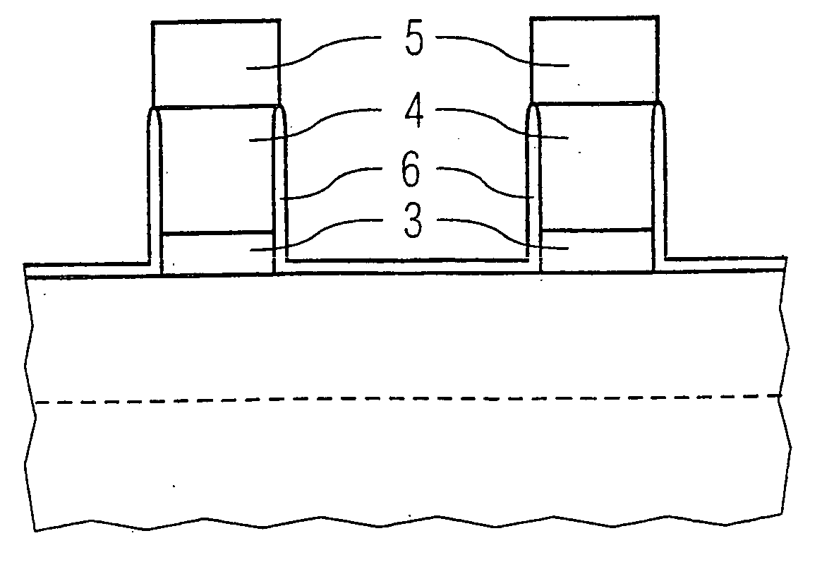
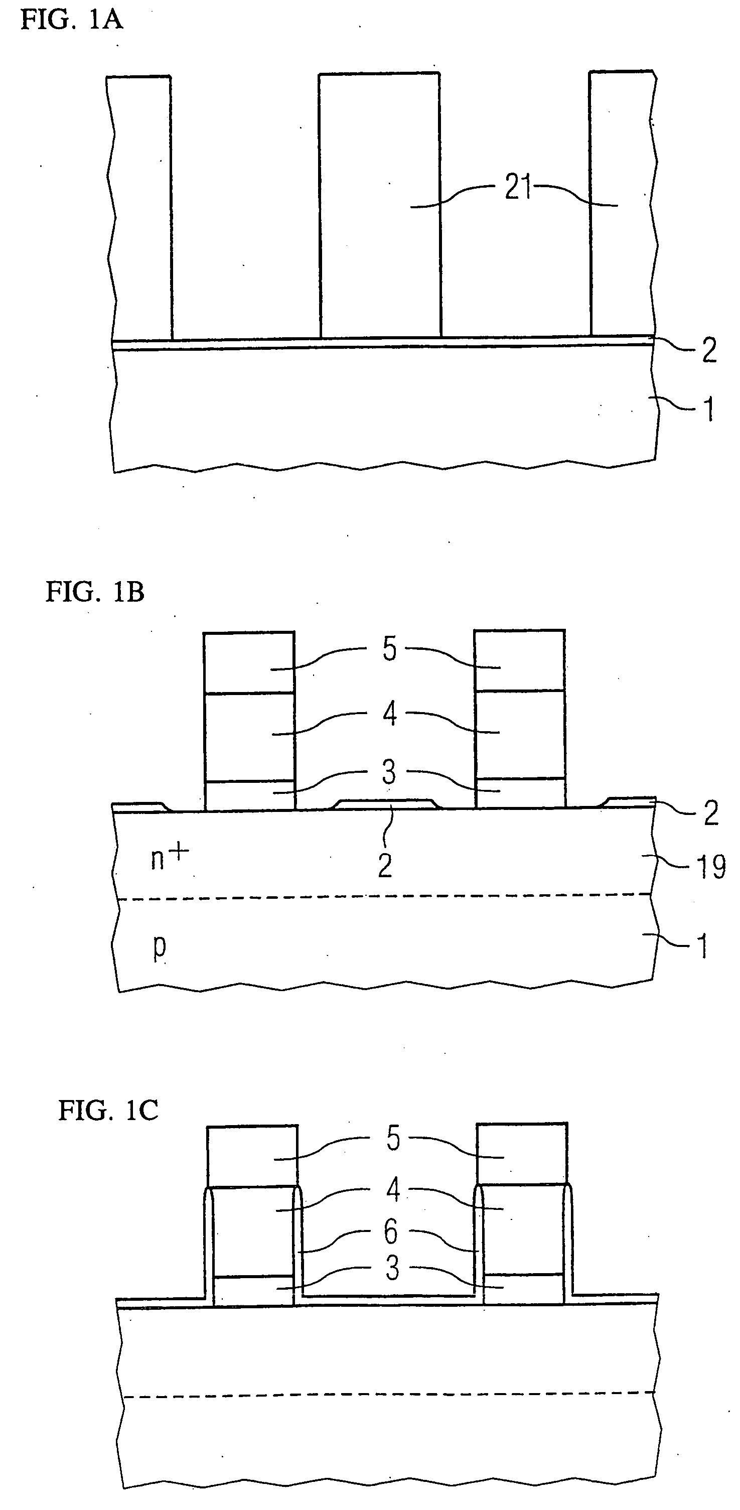
[0017] A preferred exemplary embodiment of the method begins, in accordance with the cross-section illustrated in FIG. 1A, proceeding from a semiconductor body 1 or a semiconductor layer 1 applied on a substrate, on which firstly a pad oxide / nitride 2 is applied in a manner known per se. The semiconductor body 1 preferably has a basic doping which is weakly p-conducting. At the top side provided with the pad oxide 2, an n+-doped well is formed by introduction of dopant. The pad oxide layer later serves as an etching stop layer 2. An oxide is preferred here, although in principle any material with respect to which the material of the bit line layers to be applied can be etched selectively is suitable as an etching stop layer 2.

[0018] Preferably, all STI isolations (shallow trench isolation) are fabricated at this point in the method. The STI isolations (not shown) may surround the entire memory cell array or individual blocks of the memory cell array. It is possible, in addition, to...


PUM


Abstract

An electrically conductive bit line layer is applied and patterned into portions arranged parallel to one another before the trench is etched into the semiconductor material, in which case, after the patterning of the bit line layer (3, 4) and before the etching of the trench, an implantation is introduced for the purpose of defining the position of the junctions, or, after the implantation of the n+-type well (19) for the source/drain regions, the bit line layer (3, 4) is patterned using an etching stop layer (2) arranged on the semiconductor body (1).

Description

[0001] This application is a continuation of co-pending International Application No. PCT / DE03 / 01573, filed May 15, 2003, which designated the United States and was not published in English, and which is based on German Application No. 102 25 410.9, filed Jun. 7, 2002, both of which applications are incorporated herein by reference.TECHNICAL FIELD [0002] The present invention relates to a fabrication method for NROMs with trench transistors and separate bit lines. BACKGROUND [0003] Extremely small nonvolatile memory cells are required for very large scale integration density in multimedia applications. The further development of semiconductor technology is enabling increasingly larger storage capacities which, however, are not achieved in the context of conventional fabrication technologies. [0004] DE 100 39 441 A1, which is a counterpart application to U.S. Patent Application No. 2002 / 024092, describes a memory cell having a trench transistor arranged in a trench formed at a top si...

Claims


Application Information

Patent Timeline
IPC IPC(8): H01L29/41H01L21/8242H01L21/8246H01L21/8247H01L27/115H01L29/417H01L29/423H01L29/49H01L29/788H01L29/792
CPCH01L27/11568H01L27/115H10B43/30H10B69/00H10B43/40
Inventor KLEINT, CHRISTOPHLUDWIG, CHRISTOPHWILLER, JOSEFDEPPE, JOACHIM
Owner POLARIS INNOVATIONS
Why Eureka
Try Eureka