Semiconductor device fabricating system and semiconductor device fabricating method

a technology of semiconductor devices and fabricating systems, which is applied in the direction of coatings, metallic material coating processes, chemical vapor deposition coatings, etc., can solve the problems of inability to achieve accurate flow rate control, difficult to adjust the flow rate of inert gas, and contamination of particles or gas supply lines, etc., to achieve accurate control and stably carried out

Inactive Publication Date: 2005-04-28
TOKYO ELECTRON LTD
View PDF4 Cites 20 Cited by
  • Summary
  • Abstract
  • Description
  • Claims
  • Application Information

AI Technical Summary

Benefits of technology

[0022] According to the present invention, the shutoff valves are placed in parts of the process gas supply lines close to the processing vessel, and the purge gas is supplied to parts of the process gas supply lines each extending between the shutoff valve and the processing vessel. Therefore, only the process gas remaining in the short parts of the process gas supply line extending below the shutoff valve needs to be purged in changing the proces...

Problems solved by technology

If a process gas supplied through the open gas supply line into the processing vessel flows into the other closed gas supply lines not supplying the gases, it is possible that a product is deposited in the closed gas supply lines causing contamination with particles or the gas supply lines are corroded.
Consequently, it is difficult to adjust the flow rate of the inert gas to values in a desired flow rate range and accurate flow rate control cannot be achieved.
Therefore, the total pur...

Method used


Image

  • Semiconductor device fabricating system and semiconductor device fabricating method
  • Semiconductor device fabricating system and semiconductor device fabricating method
  • Semiconductor device fabricating system and semiconductor device fabricating method

Examples


first embodiment

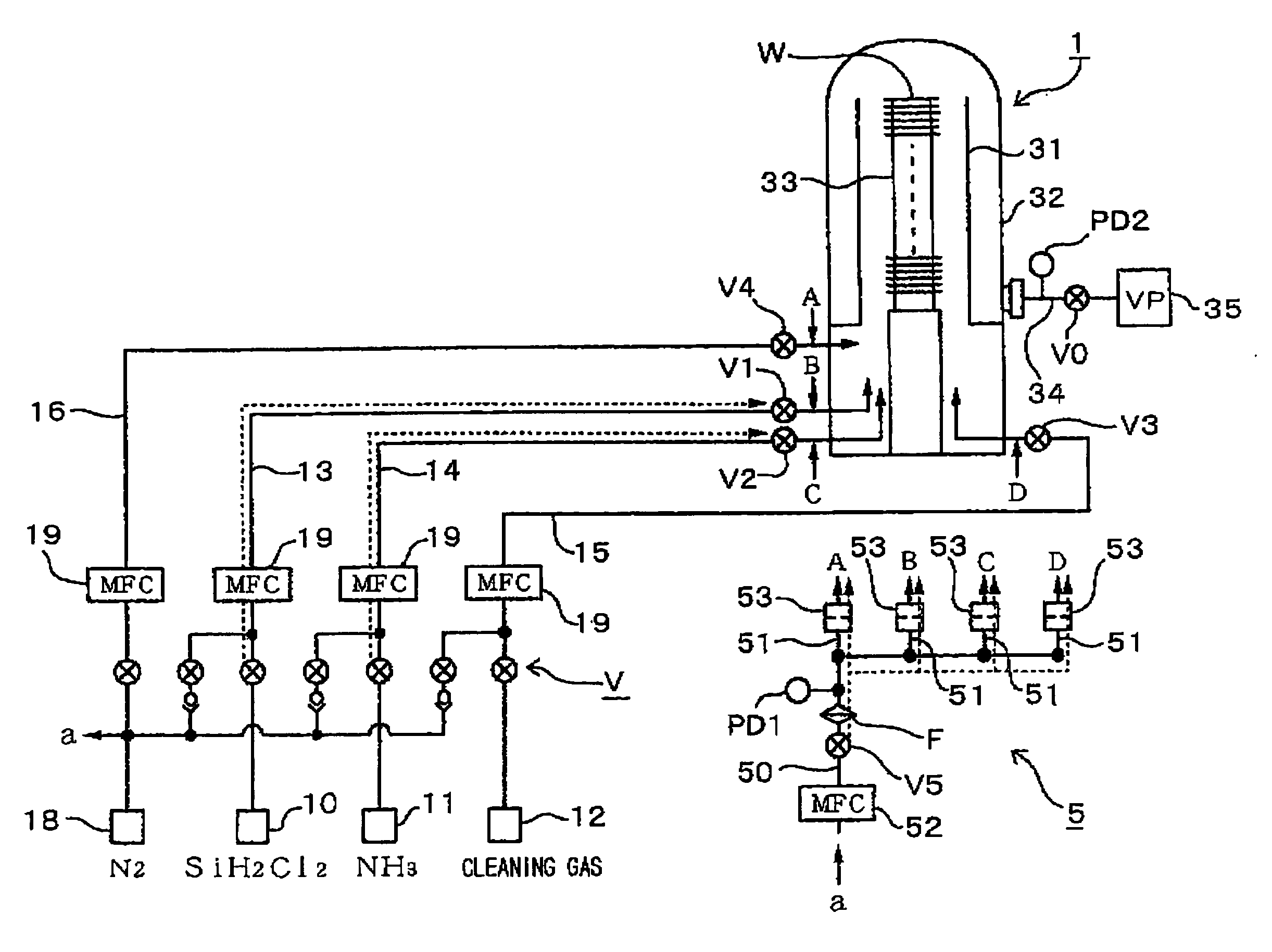
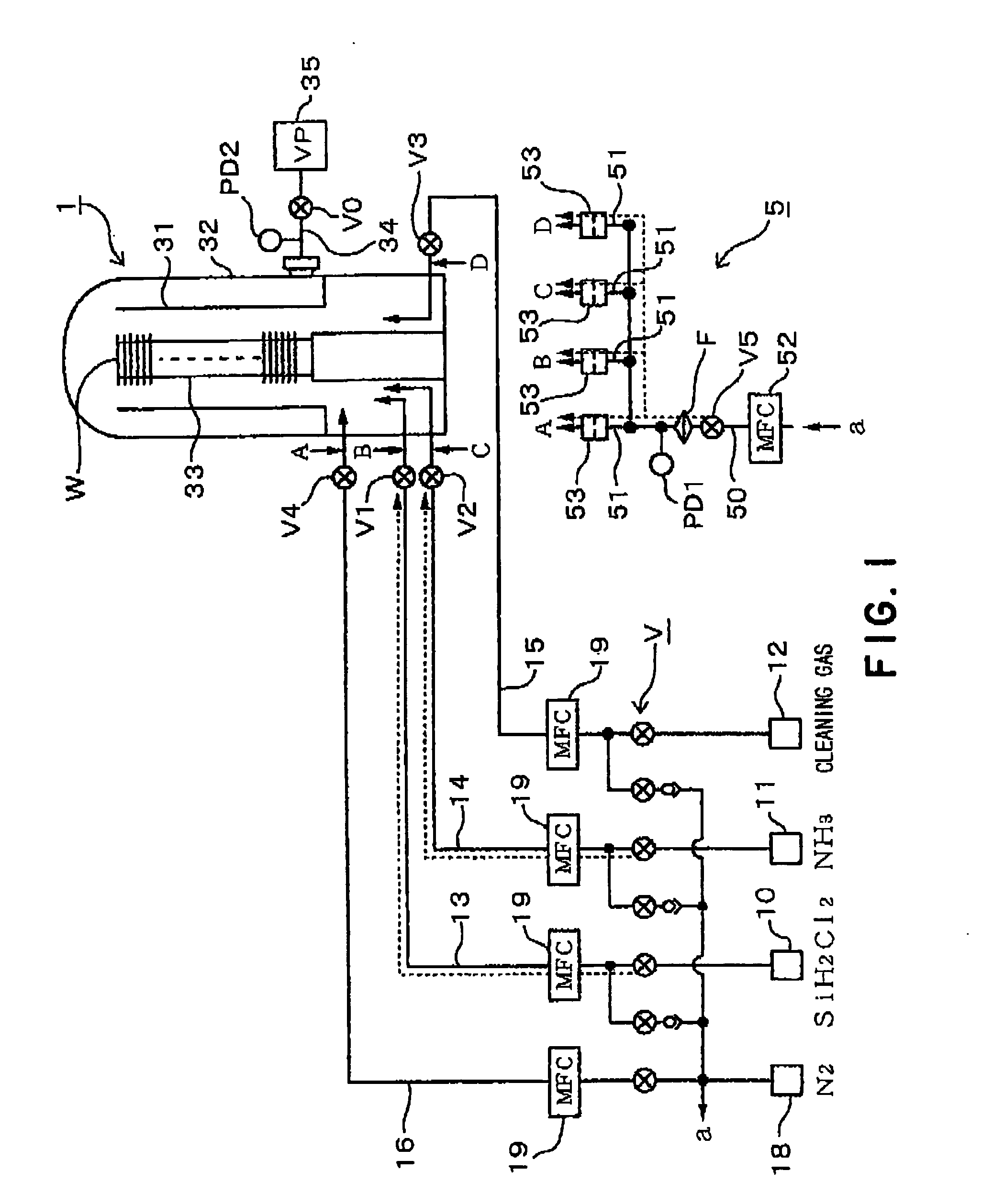
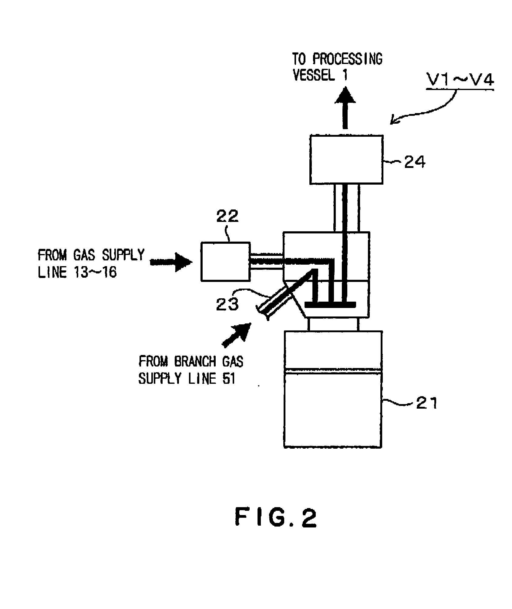
[0032]FIG. 1 shows a piping system included, in a vertical thermal processing system, namely, semiconductor device fabricating system, in a first embodiment according to the present invention. The vertical thermal processing system includes, as principal components; a processing vessel 1 for processing a semiconductor wafer, i.e., a substrate on which semiconductor devices are to be fabricated, by a thermal process, such as a film deposition process for depositing a film on the semiconductor wafer (hereinafter, referred to simply as “wafer”); three process gas sources 10, 11 and 12, i.e., a dichlorosilane source 10, an ammonia source 11 and a cleaning gas source 12; process gas supply lines 13, 14 and 15, i.e., a dichlorosilane supply line 13, an ammonia supply line 14 and a cleaning gas supply line 15, respectively connecting the process gas sources 10, 11 and 12 to the processing vessel 1; a discharge line 34 connected to the processing vessel 1; and a purge gas supply unit 5 for ...

second embodiment

[0050] A piping system included in a semiconductor device fabricating system in a second embodiment according to the present invention will be described with reference to FIG. 4. The piping system shown in FIG. 4 is provided with a flow control unit including a mass flow meter 54 and an automatic pressure regulator 55 instead of a mass flow controller for controlling the total flow rate of a purge gas flowing through branch purge gas supply lines 51. A controller, not shown, controls the automatic pressure regulator 55 arranged downstream of the mass flow meter 54 on the basis of a measured flow rate measured by the mass flow meter 54 to control the total flow rate of the purge gas for pressure control. The primary pressure on the primary side of orifices 53 is controlled to control the flow rates of the purge gas flowing through the branch purge gas supply lines 51.

third embodiment

[0051] In a piping system shown in FIG. 5 included in a semiconductor device fabricating system in a third embodiment according to the present Invention, mass flow controllers 58 are placed in branch purge gas supply lines 51, respectively, instead of the orifices 53. Since the purge gas is supplied at a low flow rate through the mass flow controllers 58 to parts of gas supply lines extending between a processing vessel 1 and shutoff valves V1 to V4 placed in the gas supply lines, the shutoff valves V placed on the gas supply lines not participating in a process may be kept closed. Therefore, the process gases used for the process and remaining in the gas supply lines can be replaced with the purge gas in a very short time before starting the next process and hence the next process can be started in a short time after the completion of the preceding process.

[0052] If the purge gas heated at temperatures in the range of, for example 100 to 200° C. by a heating device, not shown, is s...


PUM

PropertyMeasurementUnit
Pressureaaaaaaaaaa
Flow rateaaaaaaaaaa
Massaaaaaaaaaa

Abstract

Shutoff valves are placed in parts of the process gas supply lines at positions near the processing vessel. A main purge gas supply line branches into branch purge gas supply lines, each of which is provided with an orifice called sonic nozzle. The branch purge gas supply lines are connected to parts of the process gas supply lines extending between the shutoff valves and the processing vessel. The ratio P1/P2, where P1 is primary pressure on the primary side of the orifice and P2 is secondary pressure on the secondary side of the orifice, is controlled to be not less than a predetermined value, for example, two, thereby, the purge gas can always be supplied at equal flow rates into the process gas supply lines. The total flow rate of the purge gas is controlled by a mass flow controller placed in the main purge gas supply line.

Description

BACKGROUND OF THE INVENTION [0001] 1. Field of the Invention [0002] The present invention relates to a semiconductor device fabricating method of processing a substrate on which semiconductor devices are to be fabricated in a processing vessel by supplying a process gas into the processing vessel and a semiconductor fabricating system for carrying out the semiconductor device fabricating method. [0003] 2. Description of the Related Art [0004] Some semiconductor device fabricating methods carry out predetermined processes continuously to process a substrate in a processing vessel and a cleaning process for cleaning the interior of the processing vessel by selectively supplying process gases and cleaning gases through a plurality of gas supply lines connected to the processing vessel. If a process gas supplied through the open gas supply line into the processing vessel flows into the other closed gas supply lines not supplying the gases, it is possible that a product is deposited in t...

Claims


Application Information

Patent Timeline
IPC IPC(8): H01L21/02C23C16/34C23C16/44C23C16/455H01L21/3065H01L21/31H01L21/318
CPCC23C16/345H01L21/3185C23C16/455C23C16/4401H01L21/0217H01L21/02
Inventor OKABE, TSUNEYUKITAKADOU, MAKOTO
Owner TOKYO ELECTRON LTD
Why Eureka
Try Eureka