Plasma processing apparatus and method

Active Publication Date: 2005-04-28
HITACHI HIGH-TECH CORP
View PDF8 Cites 15 Cited by
  • Summary
  • Abstract
  • Description
  • Claims
  • Application Information

AI Technical Summary

Benefits of technology

[0013] The present invention has been accomplished in view of the foregoing problems, and it is an object of the present invention to provide a pla

Problems solved by technology

The non-volatile materials are difficult to etch since the melting point of the reaction products that are formed during etching is high.
Further, since the vapor pressure of the reaction products after etching is low and the deposition coefficient to the inner walls of the vacuum vessels (vacuum processing chamber) is high, the inner walls of the vacuum vessels tend to become covered with deposits of the reaction products, even after processing only a small amount of samples (several to several hundreds of sheets).
Further, when they have peeled and fallen, the deposits form obstacles.
In this process, a great amount of polymer films are deposited on the inner wall of a reactor, other than on the wafers, thereby to inhibit the mass production stability.
In any of the processing apparatuses described above, since countermeasures for the preventing formation of deposited matter on the inner wall of the vacuum vessel, in the case of etching a non-volatile material, are not completely effective, a manual cleaning operation, which involves opening the vacuum vessel to t

Method used


Image

  • Plasma processing apparatus and method
  • Plasma processing apparatus and method
  • Plasma processing apparatus and method

Examples


Embodiment Construction

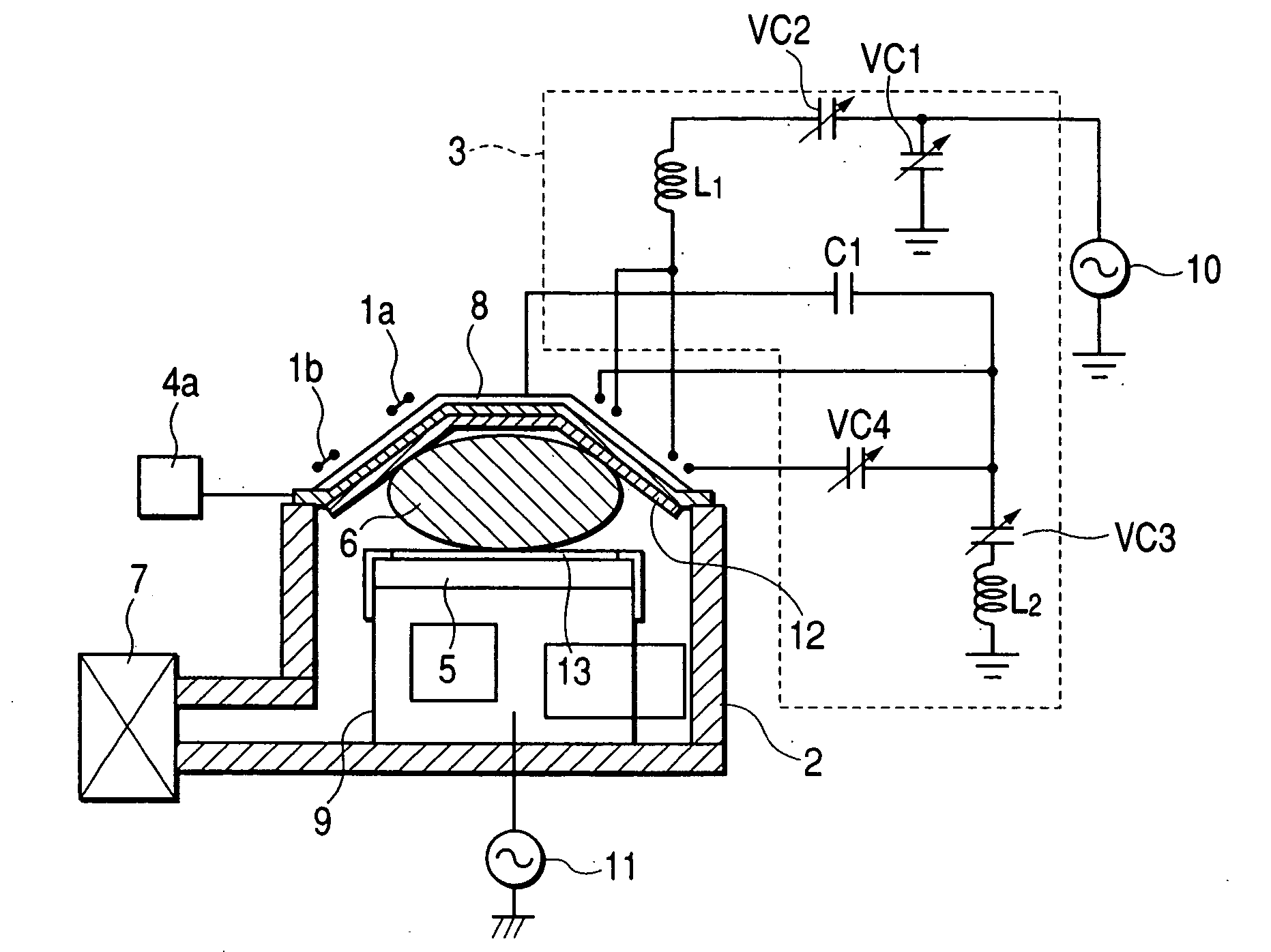
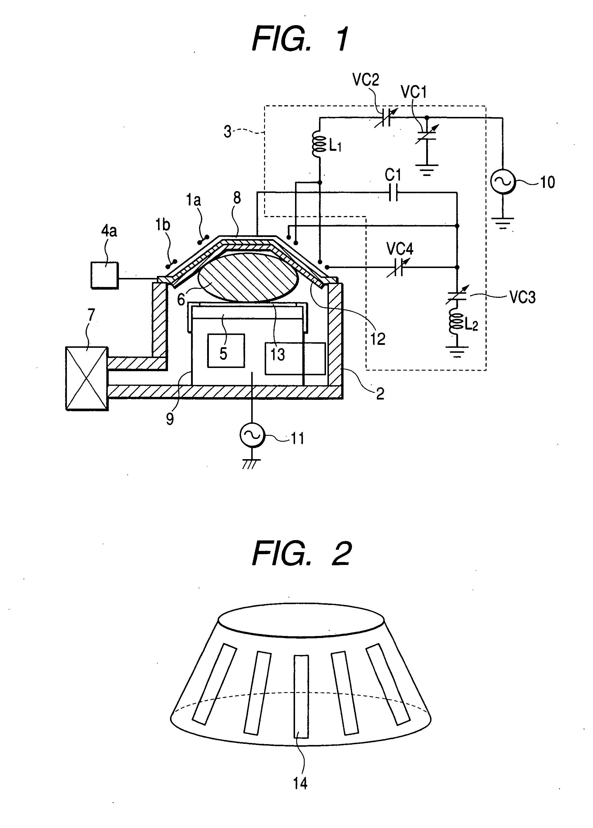
[0049] A first embodiment of the present invention will be described with reference to the drawings. In the first embodiment, a method of suppressing the deposition of reaction products, during processing, on the inner wall of a vacuum vessel will be described with reference to an example of an etching process, in a case where a sample subjected to plasma processing is made of a non-volatile material.

[0050]FIG. 1 is a cross sectional view of a plasma processing apparatus according to this embodiment. A vacuum vessel 2 has a bell jar 12, made of an insulative material (for example, a non-conductive material, such as quartz or a ceramic), which closes the upper portion of the vacuum vessel 2 so as to define a vacuum processing chamber. A sample table 5 for supporting a sample 13 to be processed is provided inside the vacuum vessel, and plasmas 6 are formed in the processing chamber to process the sample. Further, the sample table 5 is formed above a sample holding unit 9, including t...


PUM

PropertyMeasurementUnit
Electrical conductoraaaaaaaaaa

Abstract

A plasma processing apparatus includes a gas ring forming a portion of a vacuum processing chamber and having a blowing port for a processing gas, a bell jar to define a vacuum processing chamber, an antenna for supplying an RF electric field into the vacuum processing chamber to form plasmas, a sample table, a Faraday shield, and a deposition preventive plate attached detachably at least to the inner surface of the gas ring excluding the blowing port. An area of the inner surface of the gas ring including the deposition preventive plate that can be viewed from the sample surface is set to about ½ or more of the area of the sample. A susceptor made of a dielectric material covers the outer surface and the outer lateral side of the sample table. A metal film is disposed with respect to the susceptor, and an RF voltage is applied to the metal film.

Description

CROSS-REFERENCE TO RELATED APPLICATIONS [0001] This application is a continuation of application Ser. No. 10 / 378,628 filed on Mar. 5, 2003. The contents of application Ser. No. 10 / 378,628 are hereby incorporated herein by reference in their entirety.BACKGROUND OF THE INVENTION [0002] The present invention relates to a plasma processing apparatus and a plasma processing method; and, more particularly, it relates to a plasma processing apparatus and a plasma processing method with which it is possible to suppress the occurrence of obstacles caused by reaction products. [0003] Materials to be etched, which are used in the field of semiconductor device production, can include volatile materials, such as Si, Al and SiO2, for example, for a DRAM (Dynamic Random Access Memory) or logic circuit IC. Further, non-volatile materials, such as Fe, have been adopted for a FRAM (Ferroelectric Random Access Memory) or a MRAM (Magnetic Random Access Memory). [0004] The non-volatile materials are dif...

Claims


Application Information

Patent Timeline
IPC IPC(8): C23C16/44C23C16/455C23C16/458C23C16/507H01J37/32H01L21/00
CPCC23C16/4404C23C16/4558C23C16/45591C23C16/4581C23C16/507H01L21/67069H01J37/3244H01J37/32477H01J37/32495H01J37/32697H01J37/321
Inventor NISHIO, RYOJIYOSHIOKA, KENKANAI, SABUROUKANEKIYO, TADAMITSUKIHARA, HIDEKIOKUDA, KOJI
Owner HITACHI HIGH-TECH CORP
Why Eureka
Try Eureka