Thin film transistor substrate of a horizontal electric field type LCD and fabricating method thereof

a technology of thin film transistors and substrates, applied in the field of thin film transistor substrates, can solve the problems of further cost reduction and significance increase in the manufacturing cost of the liquid crystal display panel, and achieve the effects of reducing manufacturing costs, simplifying mask processes, and increasing production yield

Inactive Publication Date: 2005-05-05
LG DISPLAY CO LTD
View PDF0 Cites 28 Cited by
  • Summary
  • Abstract
  • Description
  • Claims
  • Application Information

AI Technical Summary

Benefits of technology

[0027] An object of the present invention is to provide a three-round mask process including a lift-off process that significantly simplifies the mask process, redues the manufacturing cost, and achieves the higher production yield.

Problems solved by technology

In such a liquid crystal display, the thin film transistor substrate has a complicate fabrication process leading to a significance increase in a manufacturing cost of the liquid crystal display panel.
However, since the four-round mask process still has a complicate fabricating process to limit a further cost reduction, there has been required a scheme capable of simplifying the fabricating process even further to save the manufacturing cost.

Method used


Image

  • Thin film transistor substrate of a horizontal electric field type LCD and fabricating method thereof
  • Thin film transistor substrate of a horizontal electric field type LCD and fabricating method thereof
  • Thin film transistor substrate of a horizontal electric field type LCD and fabricating method thereof

Examples


first embodiment

[0050] Hereinafter, the preferred embodiments of the present invention will be described in detail with reference to FIGS. 4 to 14. FIG. 4 is a plan view showing a structure of a thin film transistor substrate for a horizontal electric field type LCD according to the present invention, and FIG. 5 is a cross-sectional view of the thin film transistor substrate taken along lines III-III′, IV-IV′, V-V′, VI-VI′ and VII-VII′ of FIG. 4.

[0051] Referring to FIG. 4 and FIG. 5, the thin film transistor substrate includes a gate line 102 and a data line 104 provided on a lower substrate 145 intersecting each other and having a gate insulating film 146 therebetween, a thin film transistor 106 provided at an intersection of the gate line 102 and the data line 104, a pixel electrode 114 and a common electrode 118 provided at a pixel area defined by an intersection structure for forming a horizontal electric field, and a common line 116 connected to the common electrode 118. Furthermore, the thin ...

second embodiment

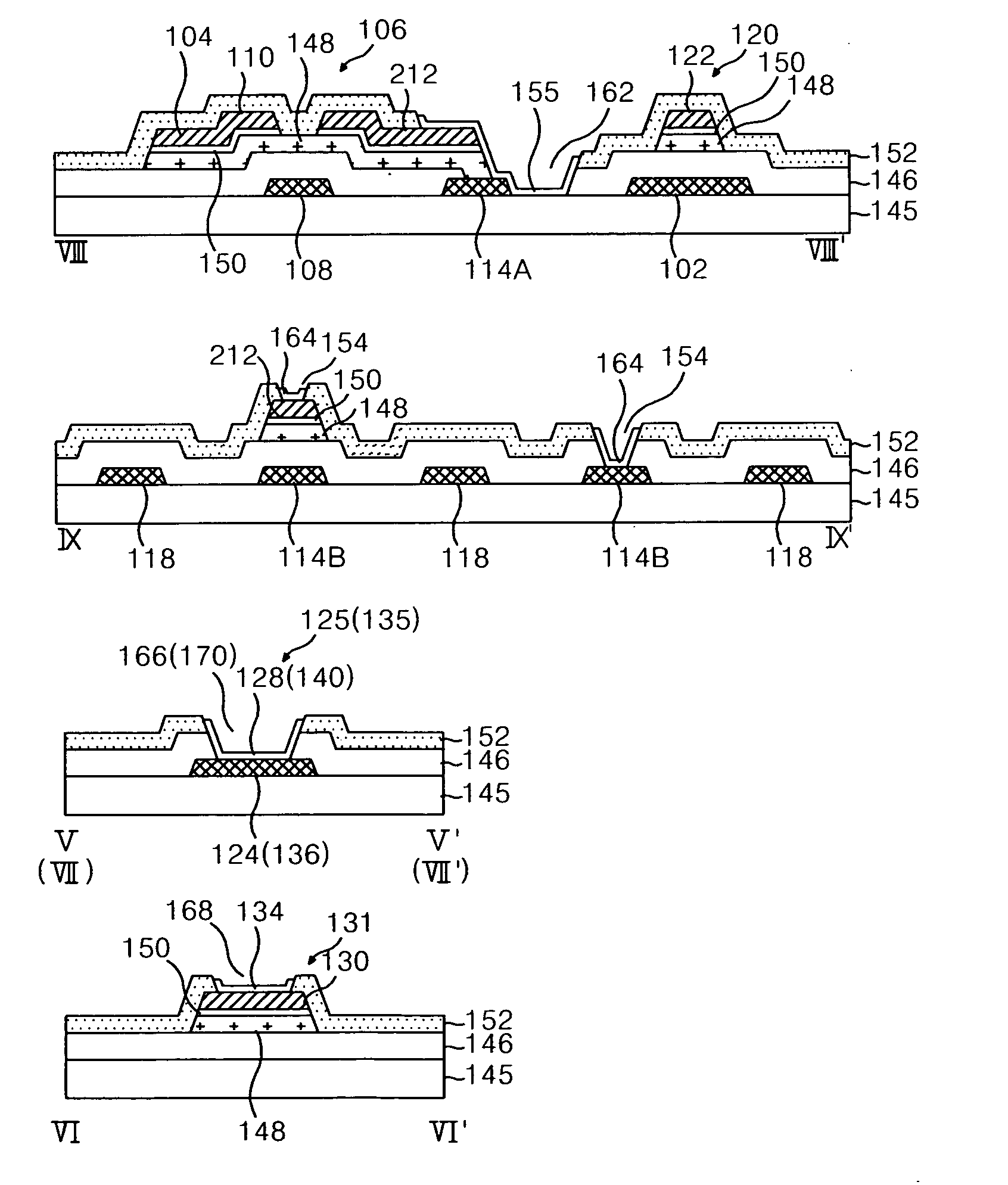
[0073]FIG. 13 is a plan view showing a structure of a thin film transistor substrate of a horizontal electric field type LCD according to the present invention. FIG. 14 is a cross-sectional view of the thin film transistor substrate taken along lines V-V′, VI-VI′, VII-VII′, VIII-VIII′ and IX-IX′ of FIG. 13. The thin film transistor substrate shown in FIG. 13 and FIG. 14 has a structure in which the second storage capacitor 126 is removed from the thin film transistor substrate shown in FIG. 4 and FIG. 5. Accordingly, a detailed explanation of the similar elements will be omitted.

[0074] A storage capacitor 120 includes a lower storage electrode formed continuous with a gate line 102, and an upper storage electrode 122 overlapping the lower storage electrode. A gate insulating film 146, an active layer 148 and an ohmic contact layer 150 are disposed between the upper storage electrode 122 and the lower storage electrode 120, and insulating each other. The upper storage electrode 122 i...


PUM

PropertyMeasurementUnit
horizontal electric fieldaaaaaaaaaa
areaaaaaaaaaaa
electric fieldaaaaaaaaaa

Abstract

A thin film transistor substrate structure of a horizontal electric field type LCD comprises a plurality of signal lines including a gate, a data, and a common lines disposed on a substrate; the data line intersecting with the gate and common lines, a gate insulating film disposed between the data line and the gate and common lines, a pixel area being defined by the intersection of the data and gate lines; a thin film transistor disposed at the intersection of the data line and gate line; a common and a pixel electrodes both having a portion extended into the pixel area; a protective film disposed over the substrate and the thin film transistor; and at least one pad structure including an upper pad electrode contacting a lower pad electrode within a first contact hole wherein the upper pad electrode is absent from the upper surface of the protective film.

Description

[0001] This application claims the benefit of the Korea Patent Application No. 2003-0077656 filed on Nov. 4, 2003, which is hereby incorporated by reference. BACKGROUND OF THE INVENTION [0002] 1. Field of the Invention [0003] The present invention relates to a liquid crystal display, and more particularly to a thin film transistor substrate structure of horizontal electric field applying type and a fabricating method thereof that are capable of simplifying a fabricating process by a three-round mask process including lift-off process. [0004] 2. Description of the Related Art [0005] Generally, a liquid crystal display (LCD) controls light transmittance of liquid crystal material using an electric field to display a picture. The liquid crystal displays are largely classified into a vertical electric field type and a horizontal electric field type depending upon the direction that the electric field drives the liquid crystal material. [0006] The vertical electric field type liquid crys...

Claims


Application Information

Patent Timeline
Patent Type & Authority Applications(United States)
IPC IPC(8): G02F1/1368G02F1/1343G02F1/1362G09F9/30H01L21/336H01L21/77H01L21/84H01L27/12H01L29/786
CPCG02F1/134363G02F1/1362H01L27/1288H01L29/66765H01L27/124G02F2001/136231G02F1/136231H01L29/786
Inventor YOO, SOON-SUNGCHANG, YOUN-GYOUNGCHO, HEUNG-LYUL
Owner LG DISPLAY CO LTD
Why Eureka
Try Eureka