CMOS image sensor and method for fabricating the same

a technology of image sensor and manufacturing method, which is applied in the manufacture of solid-state devices, semiconductor/solid-state devices, electric devices, etc., can solve the problems of high power consumption, complex driving method, and charge coupled devices (ccds) to achieve the effect of reducing darkcurren

Inactive Publication Date: 2005-05-05
COLUMBA TECH INC
View PDF20 Cites 46 Cited by
  • Summary
  • Abstract
  • Description
  • Claims
  • Application Information

AI Technical Summary

Benefits of technology

[0031] An object of the present invention is to provide a CMOS image sensor and a method for fabricating the same, which can decrease a darkcurrent at a photodiode region and a device isolation region of an image sensor.

Problems solved by technology

However, the charge coupled device (CCD) has disadvantages of a complicated driving method, high power consumption, and a complicated fabrication process requiring a multi-phased photo process.
In the charge coupled device (CCD), a control circuit, a signal processing circuit, an analog to digital (A / D) converter circuit, and so on cannot be easily integrated into a charge coupled device chip, thereby having the problem of difficulty in forming compact-size products.
However, the related art method for fabricating a CMOS image sensor has the following problems.
At the time of the n-type impurity injection into the p-type epitaxial layer for forming the photodiode region, of course, the impurities are injected into the active region, but, because the impurities are injected even to the device isolation film adjacent to the active region on which the photodiode is to be formed for some extent, there is current leakage from an interface of the active region and the device isolation film.
That is, the impurity ion injection into the interface of the active region and the device isolation film causes defects at the epitaxial layer of the interface, to produce charge or hole carriers, to provide places for reunion of the charges and the holes, thereby increasing the leakage current from the photodiode.
However, this method also fails to disclose a method for suppressing increase of the darkcurrent by preventing the impurity ions from being injected into the interface of the device isolation film and the active region for the photodiode.

Method used


Image

  • CMOS image sensor and method for fabricating the same
  • CMOS image sensor and method for fabricating the same
  • CMOS image sensor and method for fabricating the same

Examples


Embodiment Construction

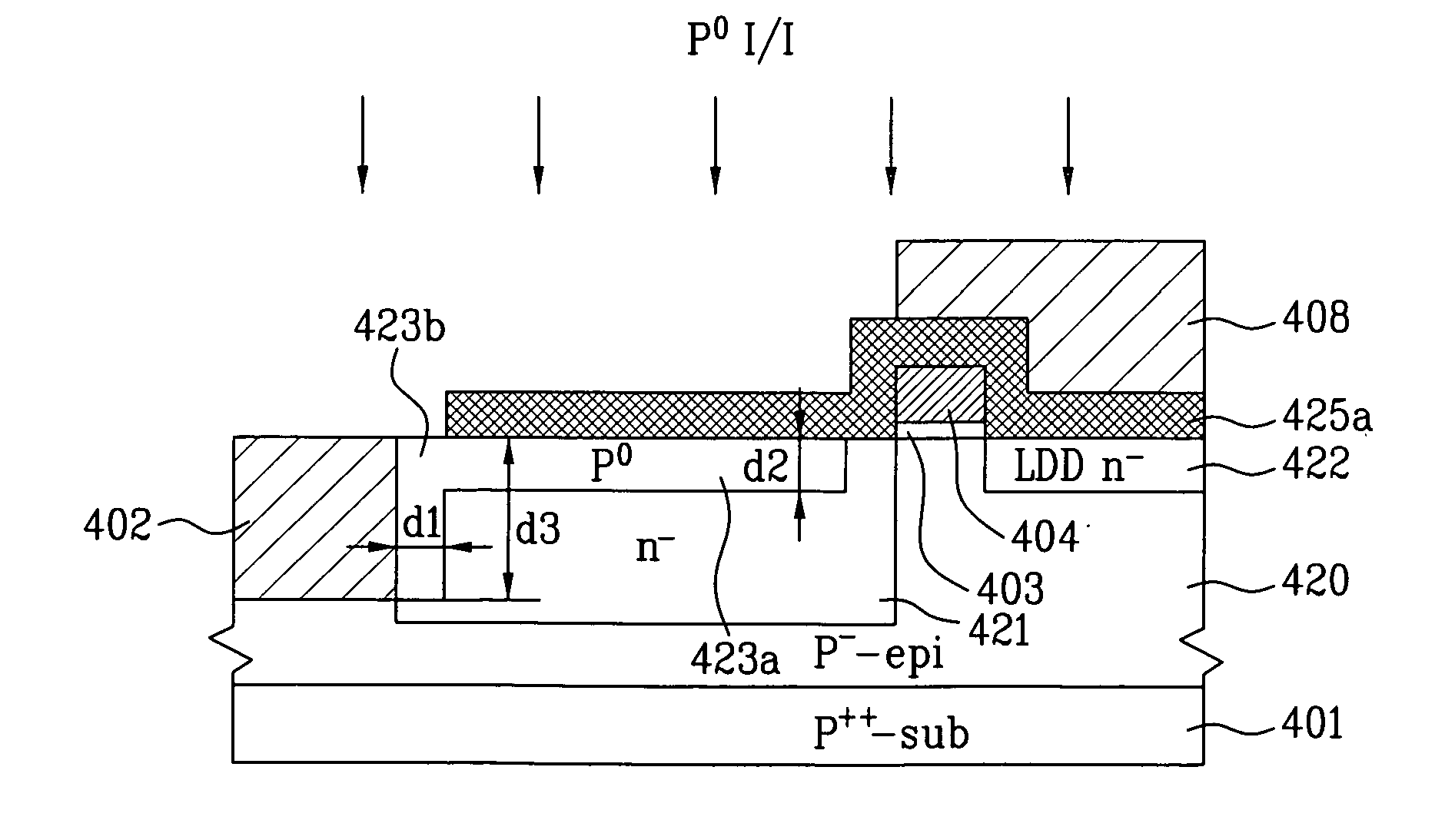
[0060] Reference will now be made in detail to the preferred embodiments of the present invention, examples of which are illustrated in the accompanying drawings. Wherever possible, the same reference numbers will be used throughout the drawings to refer to the same or like parts.

[0061]FIG. 4 illustrates a layout of a 4T-type CMOS image sensor in accordance with a first preferred embodiment of the present invention, and FIG. 5 illustrates a layout of a 3T-type CMOS image sensor in accordance with a second preferred embodiment of the present invention.

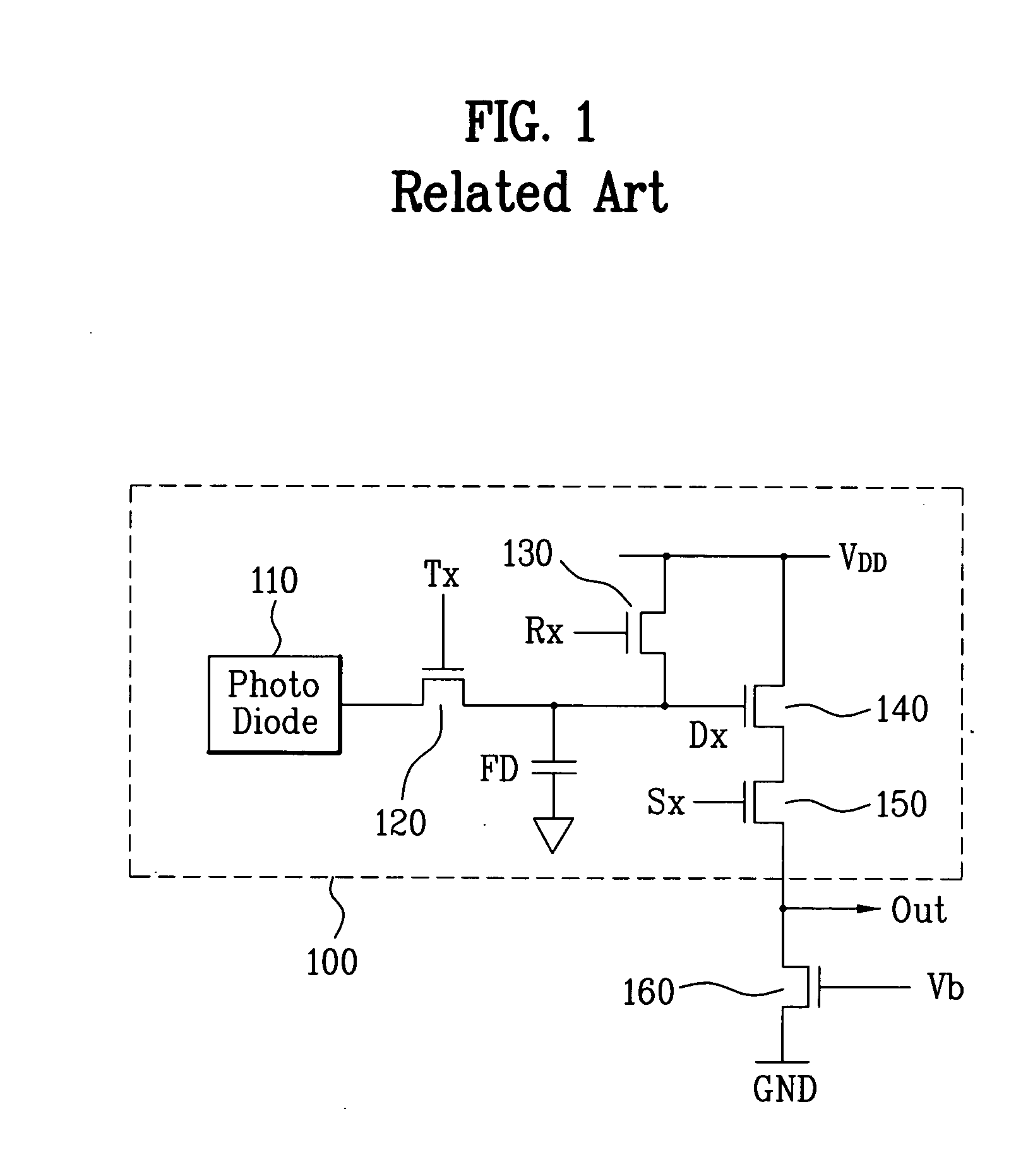
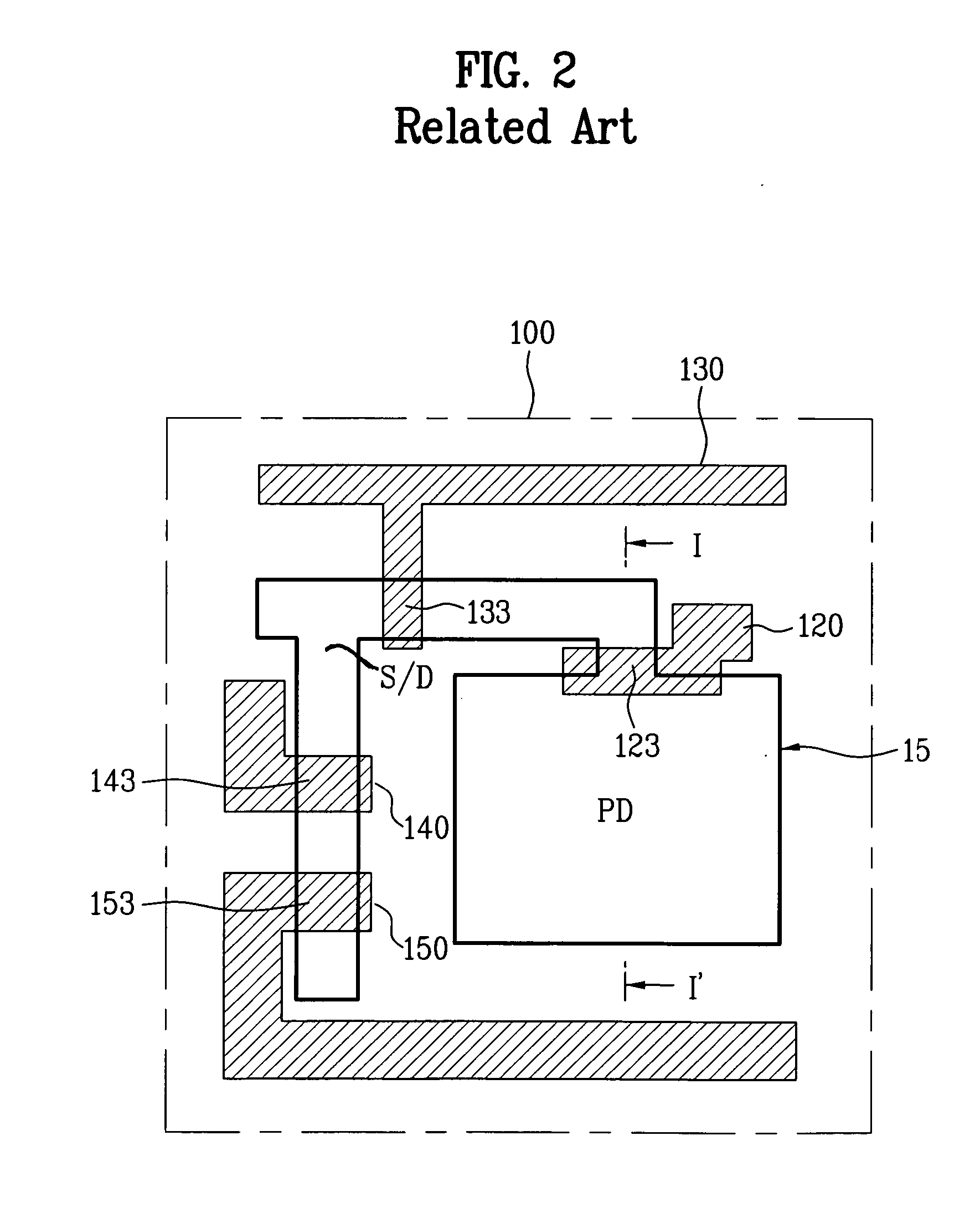
[0062] Referring to FIG. 4, a unit pixel 100 of a CMOS image sensor in accordance with a first preferred embodiment of the present invention has an active region (within a thick line) 15 defined on a substrate, and a device isolation film formed on a portion excluding the active region 15. Of the active region 15, a portion with a large width has one photodiode PD formed therein, and overlapped with rest of the active region 15, there...


PUM


Abstract

CMOS image sensor and method for fabricating the same, the CMOS image sensor including a second conductive type semiconductor substrate having an active region and a device isolation region defined therein, wherein the active region has a photodiode region and a transistor region defined therein, a device isolating film in the semiconductor substrate of the device isolation region, a first conductive type impurity region in the semiconductor substrate of the photodiode region, the first conductive type impurity region being spaced a distance from the device isolation film, and a second conductive type first impurity region in the semiconductor substrate between the first conductive type impurity region and the device isolation film, thereby reducing generation of a darkcurrent at an interface between the photodiode region and a field region.

Description

[0001] This application claims the benefit of the Korean Application Nos. P2003-77567, and P2003-77568, both filed on Nov. 4, 2003, which are hereby incorporated by reference. BACKGROUND OF THE INVENTION [0002] 1. Field of the Invention [0003] The present invention relates to CMOS image sensors, and more particularly, to a method for fabricating a CMOS image sensor which can decrease a darkcurrent generated in an interface of a photodiode region and a field region. [0004] 2. Discussion of the Related Art [0005] Generally, an image sensor is a semiconductor device for converting an optical image into an electric signal. In the image sensors, there are charge coupled devices (CCD) and complementary metal oxide semiconductor (CMOS) image sensors. [0006] The charge coupled device (CCD) is provided with a plurality of photodiodes (PD) arranged in a matrix each for converting an optical signal into an electric signal, a plurality of vertical charge coupled devices (VCCD) formed between ea...

Claims


Application Information

Patent Timeline
Patent Type & Authority Applications(United States)
IPC IPC(8): H01L21/00H01L27/146H01L31/00
CPCH01L27/14603H01L27/14689H01L27/1463
Inventor HAN, CHANG HUN
Owner COLUMBA TECH INC
Why Eureka
Try Eureka