Matching circuits on optoelectronic devices

a technology of optoelectronic devices and matching circuits, which is applied in the direction of semiconductor lasers, semiconductor/solid-state device details, instruments, etc., can solve the problems of negative affecting the performance of the transceiver, reducing the manufacturing yield, and inconsistent size and shape of the wire bond, so as to achieve the effect of optimal performance and precise and repeatable amount of inductance or capacitance to the optoelectronic devi

Inactive Publication Date: 2005-05-05
AVAGO TECH WIRELESS IP SINGAPORE PTE
View PDF9 Cites 3 Cited by
  • Summary
  • Abstract
  • Description
  • Claims
  • Application Information

AI Technical Summary

Benefits of technology

[0008] In a preferred embodiment of the present invention, the invention provides a precise and repeatable amount of inductance or capacitance to the optoelectronic device. A matching circuit is formed on the same substrate as the optoelectronic device. The matching circuit alters the frequency response of the optoelectronic device to match a driver circuit that drives the optoelectronic device. Thus, the optical transceiver can produce optimal performance within a desired frequency range.
[0009] The matching circuit adds a precise amount of inductance, capacitance, or a combination of both to alter the frequency response of the optoelectronic device. A flip-chip configuration is used to bond the optoelectronic device to the driver circuit, because the solder balls introduce only a negligible amount of parasitic capacitance and inductance into the system. Thus, variability in the parasitics from the bonding mechanism is eliminated.
[0011] In an alternate embodiment, the matching circuit can be altered after fabrication to change the frequency response of the optoelectronic device. The substrate of the optoelectronic device is designed with two bond pads as possible contact points to the matching circuit. Each bond pad is connected to a different amount of inductance. This configuration provides some flexibility in the amount of inductance that may be introduced into a system, since the decision as to how much inductance is introduced may be delayed until after the fabrication of the matching circuit.

Problems solved by technology

However, the effect of parasitic capacitances and inductances within the transceiver becomes more pronounced as the transmission frequency increases, which negatively affects the performance of the transceiver.
Unfortunately, the size and shape of the wire bonds are not consistent: some wires may arc higher than others, and some wires may be shorter than others.
This variability lowers the manufacturing yield, because the frequency response of the transceiver may no longer meet specifications. FIG. 2B shows a sample eye diagram for an optical transceiver with excessive inductance in the wire bonds between the optoelectronic device and the driver circuit.
The ringing effect in the transmitted signal makes it difficult for the receiver to determine whether the data is a one or a zero.
The flip-chip construction of FIG. 3A is also problematic.
However, a connection with too little inductance may also negatively affect the frequency response of the optical transceiver. FIG. 3B shows a sample eye diagram for an optical transceiver having too little inductance (which manifests itself in the signal as insufficient response peaking) in the wire bonds between the optoelectronic device and the driver circuit.
The transmitted signal takes much longer to complete its transitions, which slows down the speed at which data can be transmitted.
However, these methods are time-consuming, expensive, and difficult to repeat.

Method used


Image

  • Matching circuits on optoelectronic devices
  • Matching circuits on optoelectronic devices
  • Matching circuits on optoelectronic devices

Examples


Embodiment Construction

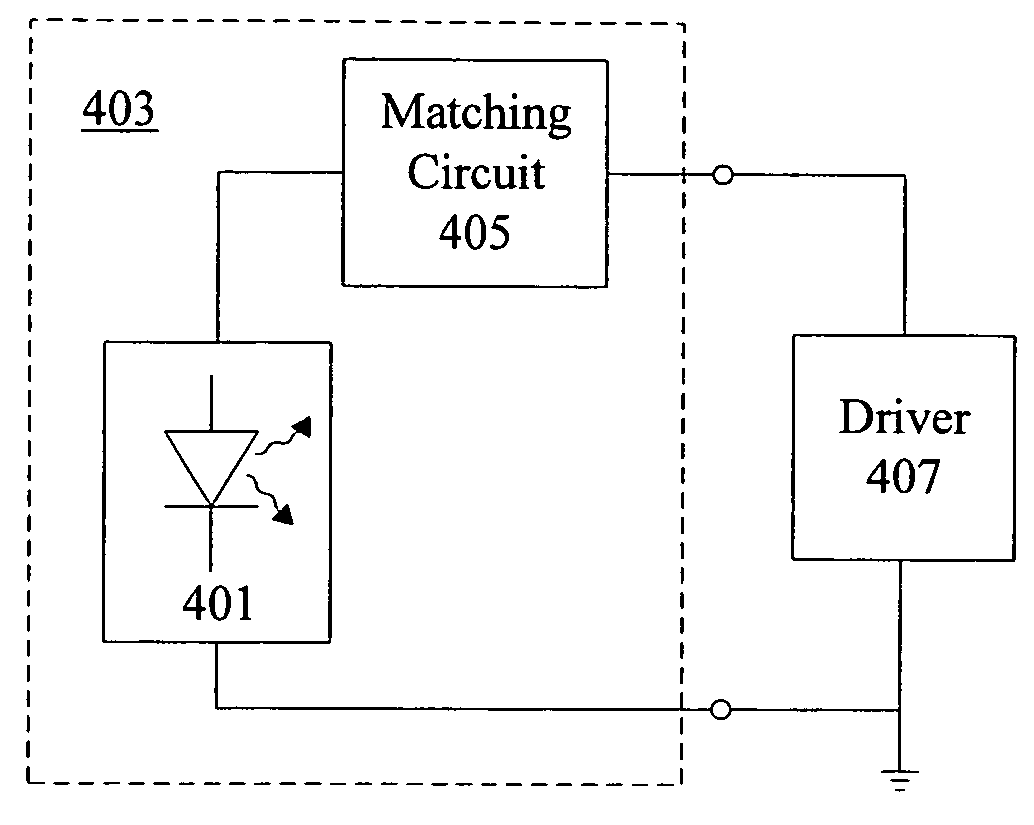
[0025]FIG. 4 shows a high-level block diagram of a preferred embodiment made in accordance with the teachings of the present invention. An optoelectronic device 401 is formed upon a substrate 403. A matching circuit 405 is formed upon the same substrate 403 and coupled to the optoelectronic device 401. A driver circuit 407 controls the output of the optoelectronic device 401. The matching circuit 405 is designed to tune the frequency response of the optoelectronic device 401 to the driver circuit 407 for optimal performance within a desired frequency range.

[0026] The matching circuit 405 introduces a precise amount of inductance, capacitance, or both to alter the frequency response of the optoelectronic device 401. The actual amount of inductance or capacitance required to produce an optimal performance may be determined empirically through circuit simulations.

[0027]FIGS. 5A-5D show possible circuit configurations for the matching circuit 405. The matching circuit 405 can be a sim...


PUM


Abstract

The present invention alters the frequency response of an optoelectronic device to match a driver circuit that drives the optoelectronic device. The optoelectronic device is formed on a first substrate. A matching circuit is also formed on the first substrate and coupled to the optoelectronic device to change its frequency response. The matching circuit provides a precise and repeatable amount of inductance to an optoelectronic device.

Description

BACKGROUND OF THE INVENTION [0001] An optical transceiver transmits and receives light signals within a fiber optic network. The light source for the transceiver is typically an optoelectronic device, such as a Vertical Cavity Surface Emitting Laser (VCSEL), a Light Emitting Diode (LED), a laser, or other light-emitting device. The light output from the optoelectronic device is controlled by a driver circuit. [0002] In digital transmissions, the driver circuit drives the optoelectronic device between high and low signal outputs to represent a digital data stream. The data is synchronized to a clock with a regular period. During a certain window of time during each clock cycle, the transmitted signal must clearly be a one or zero for the receiver to read the data correctly. Any signal transitions are done outside this window. When plotted on an oscilloscope, the transmitted signal looks like the graph in FIG. 1, known as an eye diagram. A transceiver with optimal performance has fast...

Claims


Application Information

Patent Timeline
Patent Type & Authority Applications(United States)
IPC IPC(8): G09G3/32H01L23/64H01S5/042H01S5/062H04B10/02
CPCH01S5/042H01S5/06226H01L2924/0002H01L2924/00
Inventor MAHOWALD, PETER HENRY
Owner AVAGO TECH WIRELESS IP SINGAPORE PTE
Why Eureka
Try Eureka