Fabrication method of semiconductor package with heat sink

a technology of semiconductor packaging and heat sink, which is applied in the direction of semiconductor devices, semiconductor/solid-state device details, electrical apparatus, etc., can solve the problems of limiting the improvement of heat dissipation efficiency, affecting the heat dissipation efficiency, so as to prevent the damage of bonding wires, reduce thermal stress, and prevent the effect of bonding wire damag

Inactive Publication Date: 2005-05-05
SILICONWARE PRECISION IND CO LTD
View PDF22 Cites 32 Cited by
  • Summary
  • Abstract
  • Description
  • Claims
  • Application Information

AI Technical Summary

Benefits of technology

[0009] A primary objective of the present invention is to provide a semiconductor package with a heat sink, in which the heat sink is dimensioned to maximizing an exposed surface area thereof, so as to prevent resin flash from occurrence and improve the heat-dissipating efficiency. Moreover, the semiconductor package of the invention allows the heat sink to come in direct contact with a chip for further improving the heat-dissipating efficiency, and also prevents the chip from cracking in a molding process for assuring quality of the package. Furthermore, the invention can be implemented with the heat sink being attached to the chip in a batch-type manner in no concern with height controlling, which makes the overall fabrication simplified in process and reduced in cost. In addition, molds used for the semiconductor package of the invention can also be applied to various sized products, further reducing the fabrication cost.
[0011] The combined structure of the heat sink, the chip and the chip carrier has a height smaller than that of a mold cavity of molds used in a molding process, that is, the molding resin will encapsulate the interface layer of the heat sink during molding. As the interface layer has poor adhesion to the molding resin, the molding resin on the interface layer can be easily removed after forming the encapsulant, which will not lead to delamination between the heat sink and the encapsulant due to good adhesion therebetween. Furthermore, as the heat sink does not abut a top wall of the mold cavity, there is no concern for the chip to be cracked during molding. In addition, due to certain extent in flexibility for the height of the above combined structure, the molds can be applied to semiconductor packages varied in height.
[0012] The interface layer of the heat sink can be made of a metallic material having poor adhesion to the molding resin, such as gold, chromium, nickel, alloy thereof, or Teflon, making the heat dissipation through the heat sink not undesirably affected by the interface layer.
[0015] In a further preferred embodiment of the invention, the chip carrier is a QFN (quad flat nonlead) lead frame or a BGA substrate, which has an upper surface for mounting the chip thereon and is connected to the chip through a plurality of bonding wires. In order to prevent the bonding wires from being damaged by the attachment of the heat sink to the chip, on the first surface of the heat sink there is formed a connecting portion extending toward the chip at a position corresponding to the chip. This allows the heat sink to be connected to the chip through the connecting portion without contacting the bonding wires.
[0016] In a further preferred embodiment of the invention, the chip carrier is a QFN lead frame or a BGA substrate, which has an upper surface for mounting the chip thereon and is connected to the chip through a plurality of bonding wires. In order to prevent the bonding wires from being damaged by the attachment of the heat sink to the chip, as well as reduce a thermal stress generated from the heat sink to the chip due to the difference in CTE (coefficient of thermal expansion) between the heat sink and the chip, a buffer pad having a similar CTE to that of the chip can be interposed between the heat sink and the chip. The buffer pad is preferable a defective die for optimizing the reduction in the thermal stress.
[0017] In addition, the first surface of the heat sink can be roughened, corrugated or made uneven so as to enhance the bonding strength between the heat sink and the encapsulant.

Problems solved by technology

However, as the encapsulant for enclosing the semiconductor chip is made of a molding compound e.g. epoxy resin that is poor in thermal conductivity, the heat generated by the chip is unable to be effectively dissipated through the encapsulant.
However, it is undesirable if the heat sink is entirely encapsulated by the encapsulant, in which the generated heat still needs to pass through the encapsulant for dissipation, limiting the improvement in the heat-dissipating efficiency.
Nevertheless, if the heat sink is not in direct contact with the chip, while the molding compound is filled in a space between the heat sink and the chip, the heat dissipation will be undesirably impeded due to the heat generated by the chip unable to be effectively transmitted to the heat sink.
Nevertheless, some drawbacks have been found for the semiconductor package 1 in fabrication.
However, the flash process is undesirably time-consuming and cost-ineffective, even possibly causing damage to the fabricated product.
As a result, the fabricated product can not be assured in quality as well as not cost-effective in fabrication.
Furthermore, due to lack of preciseness in the height controlling as mentioned above, the attachment of the heat sink 11 to the chip 10 can not be accomplished in a batch-type manner in the molding process for the semiconductor package 1.
This obviously increases the complexity and time consumption for the molding process.
However, in the case of the heat sink is dimensioned to be identical in surface area to the semiconductor package, if the heat sink is not precisely made, the heat sink can not be placed into the mold cavity properly when the heat sink is over-sized; while resin flash tends to occur on the top surface and side surfaces of the heat sink when the heat sink is insufficiently dimensioned.

Method used


Image

  • Fabrication method of semiconductor package with heat sink
  • Fabrication method of semiconductor package with heat sink
  • Fabrication method of semiconductor package with heat sink

Examples


first preferred embodiment

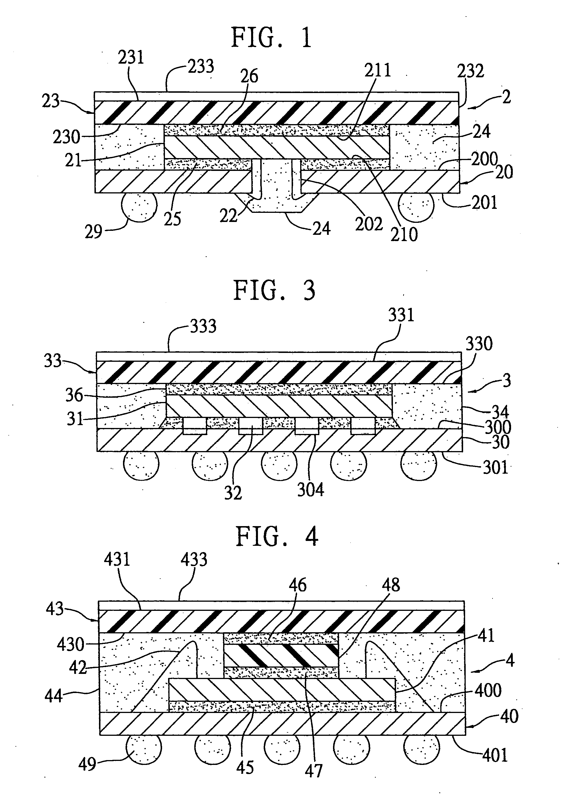
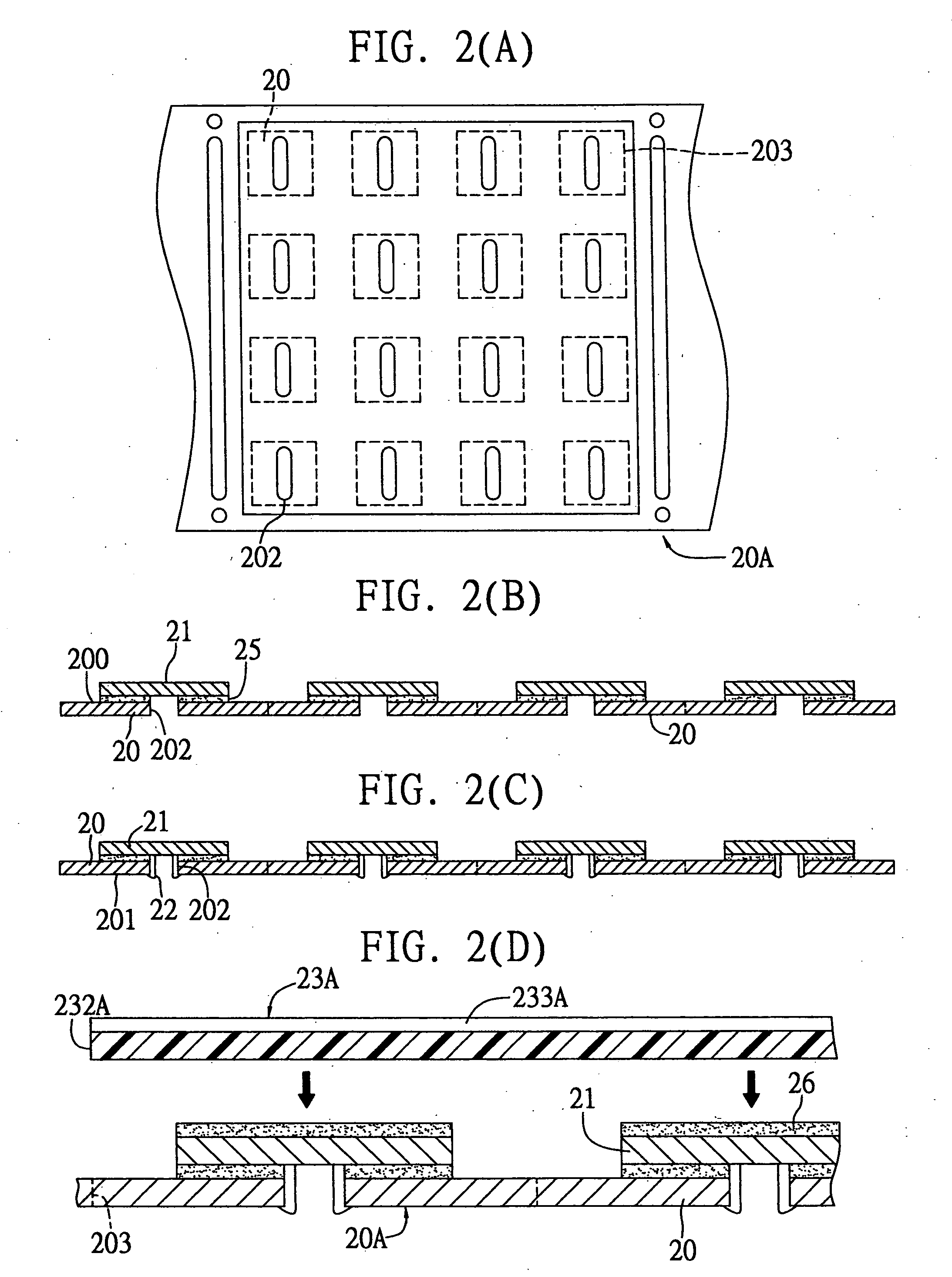
[0027] As shown in FIG. 1, a semiconductor package 2 of the first embodiment of the invention includes a substrate 20; a chip 21 mounted on the substrate 20; a plurality of gold wires 22 for electrically connecting the substrate 20 to the chip 21; a heat sink 23 attached to the chip 21; and an encapsulant 24 for encapsulating the chip 21 and gold wires 22.

[0028] The substrate 20 has an upper surface 200, a lower surface 201 opposing the upper surface 200, and a hole 202 penetrating the substrate 20. On the lower surface 201 of the substrate 20 there are formed a plurality of conductive traces (not shown), which are connected to the chip 21 by means of the gold wires 22 passing through the hole 202 for electrically connecting the substrate 20 to the chip 21. The chip 21 has an active surface 210 and an opposing inactive surface 211. The active surface 210 is attached to the upper surface 200 of the substrate 20 through an adhesive 25 such as silver paste, while a plurality of bond p...

second preferred embodiment

[0039] Illustrated in FIG. 3 is the second embodiment of the semiconductor package of the invention. The semiconductor package 3 includes a flip chip substrate 30, wherein a plurality of bump pads 304 are formed at predetermined positioned on an upper surface 300 of the substrate 30, and a plurality of conductive traces (not shown) are formed on the upper surface 300 and an opposing lower surface 301 of the substrate 30 respectively. Then, a plurality of solder lumps 32 are bonded to the bump pads 304 for electrically connecting a chip 31 to the substrate 30 in a flip chip manner through the solder bumps 32. The chip 31 is attached to a first surface 330 of a heat sink 33 through an adhesive 36, allowing heat generated by the chip 31 to be directly transmitted to the heat sink 33. Further, on a second surface 331 opposing the first surface 330 of the heat sink 33 there is coated a gold layer 333, which with a molding resin has adhesion therebetween smaller than that between the firs...

third preferred embodiment

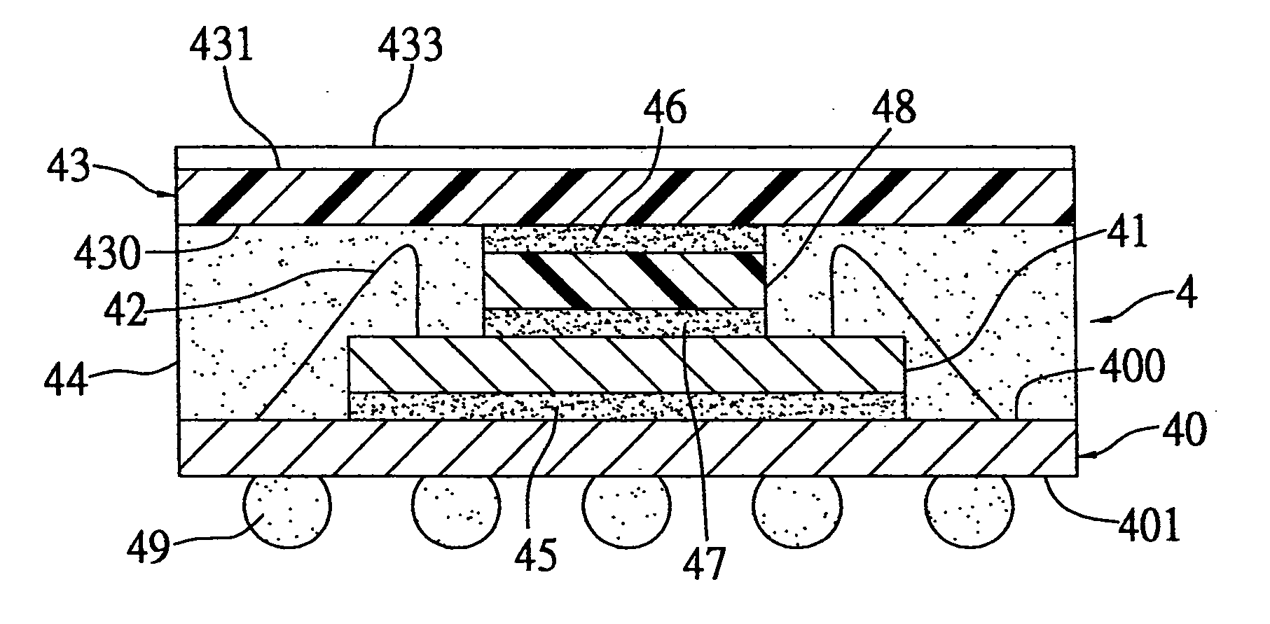
[0040] Illustrated in FIG. 4 is the third embodiment of the semiconductor package of the invention. The semiconductor package 4 adopts a conventional BGA substrate 40 having an upper surface 400 and a lower surface 401 respectively formed with a plurality of conductive traces (not shown), while the conductive traces on the surfaces 400 and 401 are electrically connected to each other. A chip 41 is attached to the upper surface 400 of the substrate 40 through an adhesive 45 such as silver paste, and then electrically connected to the substrate 40 through a plurality of gold wires 42. Subsequently, a buffer pad 48 is attached through an adhesive 47 to an approximately central position of a surface of the chip 41 having the gold wires 42 bonded thereto. The buffer pad 48 has a similar thermal expansion coefficient to the chip 41 and is dimensioned for not interfering the gold wires 42. Further, the buffer pad 48 is constructed to be higher than arcs of the gold wires 42, so as to preve...


PUM


Abstract

A semiconductor package with a heat sink is proposed, in which a chip has its first surface attached to a chip carrier, while a second surface of the chip is attached to a heat sink through an adhesive, allowing heat generated by the chip to be transmitted to the heat sink. Moreover, in a molding process, a molding resin is used to form an encapsulant for encapsulating the chip, while a top surface and side surfaces connected to the top surface of the heat sink are exposed to outside of the encapsulant, that is, the heat sink merely has its bottom surface bonded to the encapsulant. This makes the generated heat directly dissipated to the atmosphere through the heat sink. Furthermore, the top surface of the heat sink is coated with an interface layer, while adhesion between the interface layer and the molding resin is smaller than that between the heat sink and the encapsulant. This allows the molding resin remained on the interface layer to be easily removed after completing the molding process, while delamination can be prevented from occurrence between the heat sink or the chip and the encapsulant, and also the chip can be prevented from cracking due to clamping force generated during molding.

Description

FIELD OF THE INVENTION [0001] This invention relates to semiconductor packages, and more particularly, to a semiconductor package with a heat sink so as to improve the heat-dissipating efficiency. BACKGROUND OF THE INVENTION [0002] A conventional semiconductor package having a semiconductor chip encapsulated by an encapsulant is concerned with efficient dissipation of heat generated by the chip during operation, so as to assure the lifetime and quality of the semiconductor package. [0003] However, as the encapsulant for enclosing the semiconductor chip is made of a molding compound e.g. epoxy resin that is poor in thermal conductivity, the heat generated by the chip is unable to be effectively dissipated through the encapsulant. Accordingly, a metallic heat sink or heat block is incorporated in the semiconductor package for improving the heat-dissipating efficiency. However, it is undesirable if the heat sink is entirely encapsulated by the encapsulant, in which the generated heat s...

Claims


Application Information

Patent Timeline
Patent Type & Authority Applications(United States)
IPC IPC(8): H01L21/56H01L23/31H01L23/433
CPCH01L21/561H01L2224/48247H01L23/4334H01L24/32H01L24/97H01L2224/16225H01L2224/16227H01L2224/32225H01L2224/48091H01L2224/48227H01L2224/4824H01L2224/73204H01L2224/73215H01L2224/73253H01L2224/73265H01L2224/97H01L2924/01013H01L2924/01029H01L2924/01047H01L2924/01079H01L2924/01082H01L2924/15311H01L24/48H01L2924/01005H01L2924/01006H01L2924/01024H01L2924/01033H01L2924/0132H01L2224/45144H01L2224/32245H01L23/3128H01L2924/00014H01L2224/85H01L2224/83H01L2924/01028H01L2924/00H01L2924/3512H01L2924/00012H01L24/45H01L24/73H01L2224/2612H01L2924/181H01L2924/351H01L2224/05599
Inventor HUANG, CHIEN-PINGHO, TZONG-DAHSIAO, CHENG-HSU
Owner SILICONWARE PRECISION IND CO LTD
Why Eureka
Try Eureka