Radiation detector and radiation apparatus

a radiation detector and radiation apparatus technology, applied in the direction of x/gamma/cosmic radiation measurement, radioation controlled devices, instruments, etc., can solve the problems of signal detection delay unavoidably, large weakened electric field outside the grid electrode, and shorten the mean life distance of electrons, so as to improve detection efficiency and energy resolution, and collect charge quickly and efficiently

Inactive Publication Date: 2005-05-12
HITACHI LTD
View PDF8 Cites 19 Cited by
  • Summary
  • Abstract
  • Description
  • Claims
  • Application Information

AI Technical Summary

Benefits of technology

[0015] According to an 11th aspect of the invention, there are provided a radiation detector comprising a semiconductor element irradiated for generating the charge, an anode formed on the semiconductor element, a cathode formed on the semiconductor element, a plurality of independent grid electrodes formed on the semiconductor element in the neighborhood of the anode in such a ma

Problems solved by technology

According to the prior art described above, however, the electric field outside the grid electrode is greatly weakened in the neighborhood of the surface of the anode.
In this area, it takes a long

Method used


Image

  • Radiation detector and radiation apparatus
  • Radiation detector and radiation apparatus
  • Radiation detector and radiation apparatus

Examples


Embodiment Construction

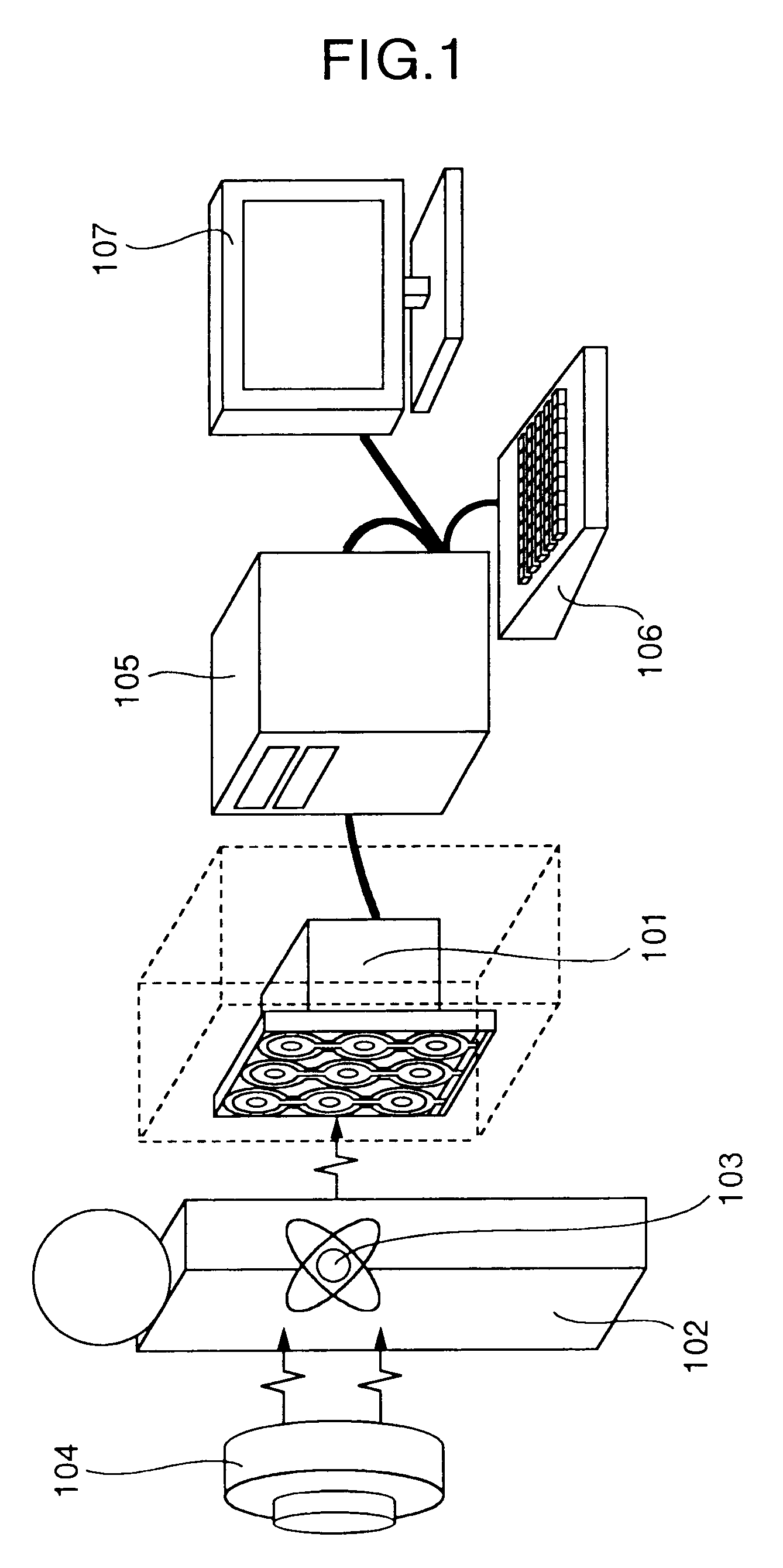
[0037] The present invention will be described below in detail with reference to embodiments thereof. FIG. 1 shows a configuration of a multiple-grid electrode radiation detector according to the invention. A multiple-grid electrode radiation detector 101 detects the radiation generated from a radio isotope 103 dosed in a human body 102 or a radiation generator 104. The radio isotope 103 includes F-18 contained in FDG (fluorodeoxy glucose) or Tc-99m contained in Neurolite (99 mTc-ECD) having a chemical form concentrated in the seat of a disease in the human body. The radiation generator 104 includes an X-ray generator. The multiple-grid electrode radiation detector 101 is connected to a data collection-analyzer 105 in a subsequent stage, and together with an input / output device 106 and an imaging / display device 107, makes up a radiation imaging system.

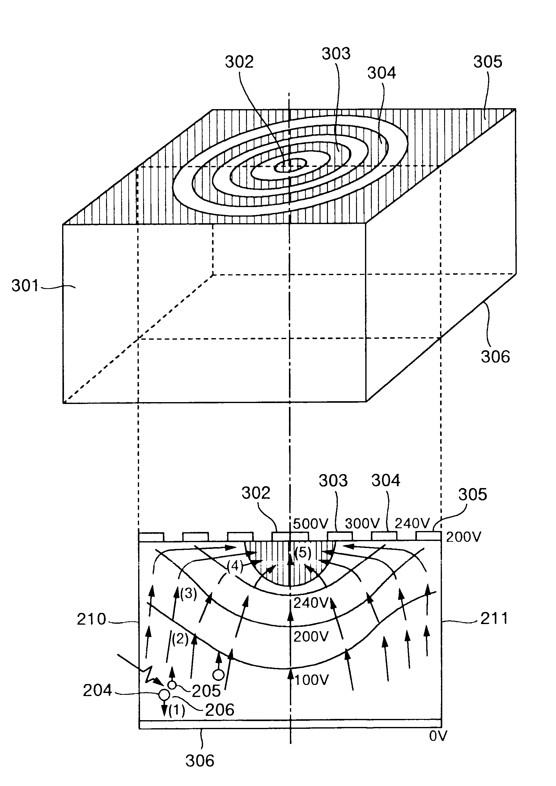
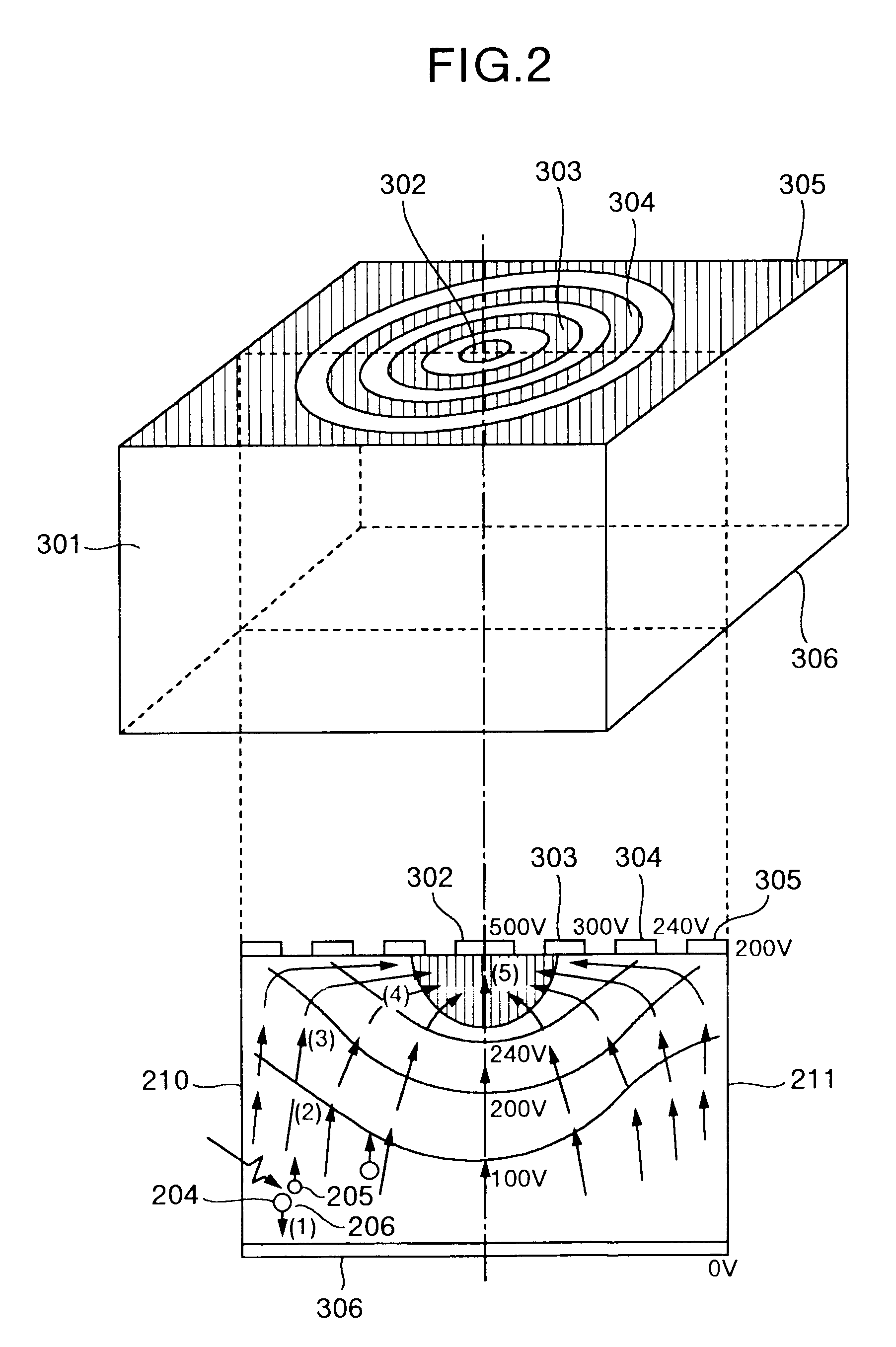
[0038]FIGS. 2 and 3 show the detail of a multiple-grid electrode radiation detector. The multiple-grid electrode radiation detector ...


PUM


Abstract

A practical semiconductor radiation detector capable of collecting electrons rapidly with a large volume is disclosed. A multiple layers of grid electrodes around an anode formed on a semiconductor element limits the generation of the induced charge signal for the anode to the space in the neighborhood of the anode, while at the same time making it possible to collect the electrons rapidly. As a result of limiting the space for generating the induced charge by the grid electrodes, the energy resolution is improved even for a thick semiconductor element. Also, the capability of rapidly collecting the electrons due to the high field strength generated by the grid electrodes makes a sensitive volume of the whole semiconductor and thus achieves a high radiation detection efficiency.

Description

BACKGROUND OF THE INVENTION [0001] The present invention relates to a radiation detector and a radiation apparatus. [0002] In recent years, the ionizing radiation has been detected mainly by use of a semiconductor element. The radiation is transformed into positive holes and electrons by the semiconductor element. A cathode and an anode are formed on the surface of the semiconductor element, and the positive holes and the electrons are detected by applying a voltage between the cathode and the anode. Specifically, an electric field is formed between the cathode and the anode, and the positive holes and the electrons are moved toward the cathode and the anode, respectively. With the movement of the positive holes and the electrons, the voltages induced in the cathode and the anode are detected. [0003] The electrons and the positive holes have a mean life unique to the base material of the semiconductor. Especially, the positive holes tend to are extinguished within a comparatively sh...

Claims


Application Information

Patent Timeline
IPC IPC(8): H01L27/14G01T1/24H01L27/146H01L31/0224H01L31/0352H01L31/09
CPCH01L27/14603H01L27/14658G01T1/241H01L31/022408H01L31/0352H01L27/14659H01L2224/05555H01L2224/48227
Inventor YOKOI, KAZUMAKITAGUCHI, HIROSHIUMEGAKI, KIKUOAMEMIYA, KENSUKEUENO, YUUICHIROUYANAGITA, NORIHITOKOJIMA, SHINICHI
Owner HITACHI LTD
Why Eureka
Try Eureka