Nitride semiconductor device

a technology of semiconductor devices and nitride, which is applied in the direction of semiconductor devices, semiconductor lasers, lasers, etc., can solve problems such as device destruction, and achieve the effects of long life, high power output, and long li

Inactive Publication Date: 2005-05-12
NICHIA CORP
View PDF29 Cites 39 Cited by
  • Summary
  • Abstract
  • Description
  • Claims
  • Application Information

AI Technical Summary

Benefits of technology

[0012] Though, in a conventional multiple quantum well-type (hereinafter referred to as MQW-type) nitride semiconductor device, all the barrier layers are, in general, doped with an n-type impurity, such as Si, in order to enhance light emission efficiency by increasing the initial electron concentration in the active layer, a nitride semiconductor device of the present invention has a barrier layer, that is doped with an n-type impurity in the same manner as in the prior art, while an n-type impurity is not substantially included only in the first barrier layer that is nearest to the p-type nitride semiconductor layer. In such a structure, characteristics with respect to the device lifetime and the reverse withstanding voltage of the nitride semiconductor device can be improved.
[0047] (23) The above described p-type nitride semiconductor layer has a first p-type nitride semiconductor layer that contacts the above described active layer and becomes an electron confining layer and the active layer has a well layer of which the distance dB from the first p-type nitride semiconductor layer is in the range of from no less than 100 Å to no more than 400 Å and has a first barrier layer within the distance dB and, thereby, a nitride semiconductor device of which the device lifetime is excellent can be gained. This can be made to be a device structure wherein, as shown in FIG. 8, the distance dB from the first p-type nitride semiconductor layer 28 has a first barrier layer, that is to say, a barrier layer that does not substantially have an n-type impurity or that is adjusted to have a p-type impurity and, thereby, device deterioration due to the first p-type nitride semiconductor layer, which is a p-type carrier confining layer, is prevented so as to improve the device lifetime and it becomes possible to accelerate a light emitting recombination in a well layer arranged outside of the distance dB. Here, the device has, at least, the above described first barrier layer in the region of the distance dB, that is to say, the device has an impurity adjusted region, wherein, as described above, an impurity, or the amount of the impurity, is adjusted in at least a portion thereof in the region of the distance dB. At this time, the distance dB is preferably the first barrier layer, that is to say, a first barrier layer of which the film thickness is dB is preferably formed so as to contact the first p-type nitride semiconductor layer so that the above described effects can be maximally gained. In this manner, by using the region of the distance dB as an impurity adjusted region, as shown in FIG. 8B, a structure can be gained wherein a plurality of layers of different band gap energies are provided. For example, in FIG. 8B a region 4, of which the band gap energy is smaller than that of the barrier layer 2c, is formed wherein the above described effects can be gained by making the region dB an impurity adjusted region. Contrarily, in a similar manner, a layer 4, which has band gap energy larger than that of the barrier layer 2b, may be provided. That is to say, in the case that a plurality of layers of which the band gap energies are different are provided in the region dB, a device of which the characteristics are excellent can be gained by adjusting the impurity, or the amount of the impurity, in the region dB which is used as the first barrier layer. Furthermore, the distance dB is preferably in the range of from no less than 120 Å to no more than 200 Å so that a nitride semiconductor device with an appropriate active layer in the device structure can be gained.

Problems solved by technology

Weak reverse withstanding voltage of the devices using nitride semiconductor, which has been a problem in the part art, has a high probability of leading to destruction of the device during handling in the manufacturing process and mounting on an end product, and is therefore one of the most important problems.

Method used


Image

  • Nitride semiconductor device
  • Nitride semiconductor device
  • Nitride semiconductor device

Examples


embodiment 1

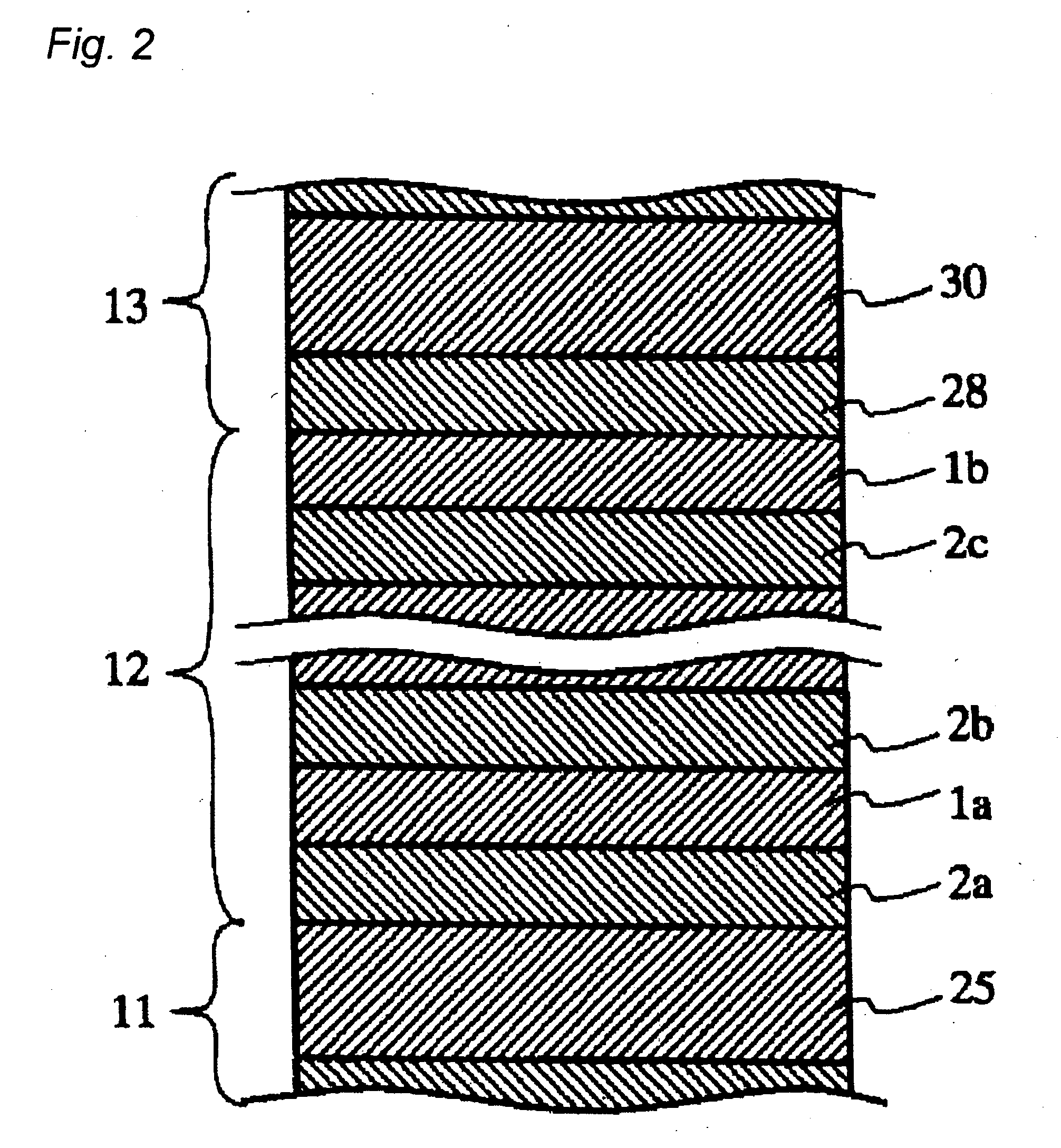
[0080] The first embodiment of the nitride semiconductor device according to the present invention comprises, as shown in FIG. 2 and FIG. 3, an active layer 12 sandwiched by a p-type nitride semiconductor layer 13 and an n-type nitride semiconductor layer 11, with the active layer including therein a first barrier layer located at a position nearest to the p-type nitride semiconductor layer and a second barrier layer which includes n-type impurity. The first barrier layer is undoped with the n-type impurity, or has been grown without doping so that substantially no n-type impurity is included therein. For the first barrier layer, either the layer nearest to the p-type nitride semiconductor layer in the active layer (hereinafter referred to as the layer nearest to the p side) may be a well layer 1b as shown in FIG. 2, or this layer may be first barrier layer as shown in FIG. 3. Preferably, as shown in FIG. 3, when the layer nearest to the p side in the active layer is used the first ...

embodiment 2

[0085] In the second embodiment of the present invention, the active layer has L (L≧2) barrier layers and, with a barrier layer located at a position nearest to the n-type nitride semiconductor layer denoted as B1 and a barrier layer which is the ith (i=1, 2, 3, . . . , L) layer from said barrier layer B1 to said p-type nitride semiconductor layer side denoted as barrier layer Bi, the barrier layers Bi of i=1 to i=n (1L of i=L does not substantially include n-type impurity. The barrier layer BL corresponds to the first barrier layer of the first embodiment and is the barrier layer located nearest to the p side, while the action of the barrier layer BL is similar to that of the first embodiment. Therefore, the barrier layer BL in the second embodiment contains at least the p-type impurity and preferably does not substantially include the n-type impurity, so that the p-type carrier is injected selectively into the barrier layer BL, thereby making the efficient injection of the carrier...

embodiment 3

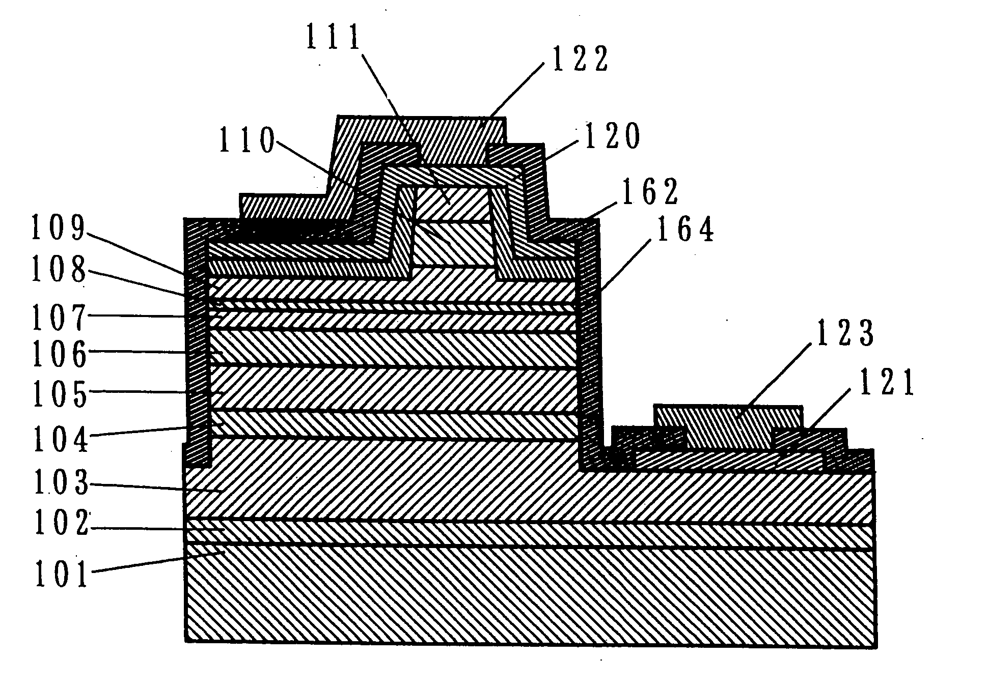
[0088] The active layer 107 has MQW structure wherein Inx1Ga1-x1N well layer (01x2Ga1-x2N barrier layer (0≦x21>x2) are stacked alternately a proper number of times in the order of barrier layer, well layer, barrier layer, with both ends of the active layer being the barrier layers. The well layers are grown undoped. On the other hand, all barrier layers except for the last barrier layer which adjoins the p-type electron confinement layer 108 are doped with an n-type impurity such as Si or Sn, while the first barrier layer is grown undoped. The last barrier layer includes a p-type impurity such as Mg which has diffused therein from the adjacent p-type nitride semiconductor layer.

[0089] As the barrier layers except for the first barrier layer are doped with the n-type impurity, the initial electron density in the active layer becomes higher and the efficiency of injecting electrons into the well layer is increased, thus resulting in improved efficiency of laser emission. The last bar...


PUM


Abstract

A nitride semiconductor device includes an n-type semiconductor layer, p-type semiconductor layer and an active layer of a quantum well structure that is sandwiched between said p-type and n-type nitride semiconductor layer, wherein the active layer has a first barrier layer, a second barrier layer and a third barrier layer. The first barrier layer is nearest to the p-type nitride semiconductor layer among the first, second and third barrier layers. The second barrier layer is nearest to the n-type nitride semiconductor layer among the first, second and third barrier layers. The third barrier layer is between the first and second barrier layers, and includes an upper barrier layer that contacts with a p-side surface of the well layer and a lower barrier layer that contacts with an n-side surface of said well layer. The upper and lower barrier layers having different composition or impurity concentrations.

Description

BACKGROUND OF THE INVENTION [0001] 1. Field of the Invention [0002] The present invention relates to a nitride semiconductor device which uses a nitride semiconductor (InxAlyGa1-X-YN, 0≦X, 0≦Y, X+Y≦1) used in light emitting devices such as light emitting diode device (LED) and laser diode device (LD), light receiving devices such as solar cell and optical sensor or electronic devices such as transistor and power devices, and particularly to a nitride semiconductor device comprising nitride semiconductor layer which includes In. [0003] 2. Description of the Prior Art [0004] Recently semiconductor laser devices which use nitride semiconductor have been receiving increasing demands for the applications in optical disk systems such as DVD which are capable of recording and reproducing a large amount of information with a high density. Accordingly, vigorous research efforts are being made in the field of semiconductor laser device which uses nitride semiconductor. Because of the capabili...

Claims


Application Information

Patent Timeline
Patent Type & Authority Applications(United States)
IPC IPC(8): H01L33/06H01L33/24H01L33/30H01L33/32H01S5/20H01S5/30H01S5/34H01S5/343
CPCB82Y20/00H01S5/343H01L33/24H01L33/32H01S5/18308H01S5/18369H01S5/2009H01S5/22H01S5/305H01S5/3054H01S5/3086H01S5/3407H01S5/3415H01S5/34333H01S2304/12H01L33/06
Inventor KOZAKI, TOKUYA
Owner NICHIA CORP
Why Eureka
Try Eureka